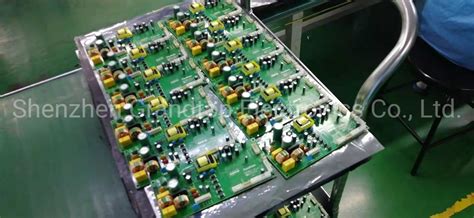
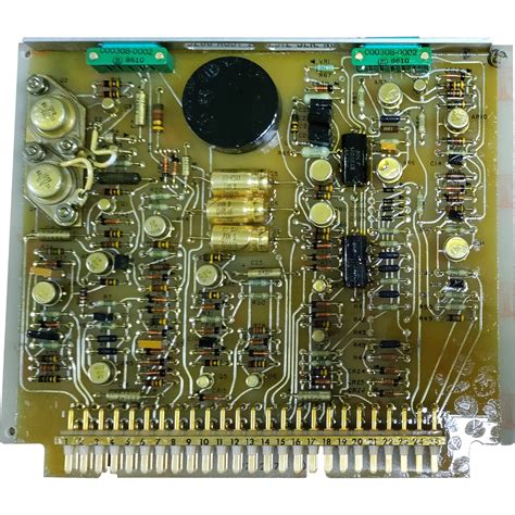
Excellent PCB engineers must have these 7 good habits
In some people’s opinion, the work of PCB layout engineers is a bit boring. Every day, they have to deal with thousands of traces on the board, various packages, and repeat the work of pulling wires… In fact, it is not as simple as it seems. Designers have to make trade-offs between various design rules, taking into account performance, process, cost and other aspects, and at the same time pay attention to the reasonable and neat layout of the board. As an excellent PCB layout engineer, good work habits will make your design more reasonable, better performance, and easier production. The following lists the 7 good habits of PCB layout engineers. Let’s see how many of them you have!

1 Learn to design rules
In fact, not only advanced PCB design software needs to set wiring rules, but some simple and easy-to-use PCB tools can also set rules. After all, the human brain is not a machine, so it is inevitable that there will be negligence and mistakes. So set some easily overlooked problems into the rules, let the computer help us check, and try to avoid making some low-level mistakes. In addition, perfect rule settings can better standardize the subsequent work. As the saying goes, sharpening the knife does not delay the chopping of wood. The more complex the scale of the board, the more important the rule setting is.
2.Execute DRC (design rules) as much as possible.
Although it only takes a short time to run the DRC function on the PCB software, in a more complex design environment, you can save a lot of time as long as you always perform checks during the design process. This is a good habit worth maintaining. Every routing decision is critical, and running DRC can remind you of the most important routing at any time. 3. Draw a good schematic diagram. Many engineers think that layout work is more important. The schematic diagram is used to generate a netlist to facilitate PCB inspection. In fact, the schematic diagram will play a greater role in the subsequent circuit debugging process. Whether it is to find problems or communicate with colleagues, the schematic diagram is more intuitive and convenient. In addition, develop the habit of marking in the schematic diagram, marking the problems that need to be paid attention to when laying out each part of the circuit on the schematic diagram, which is a good reminder for yourself or others. Hierarchical schematic diagrams divide circuits with different functions and modules into different pages, so that whether it is reading the diagram or reusing it later, it can significantly reduce the workload.

4. Optimize PCB layout. Impatient engineers can’t wait to put the components in place and start pulling wires after drawing the schematic diagram and importing the netlist into the PCB. In fact, a good PCB layout can make your subsequent wire pulling work easier and make your PCB work better. Each board will have a signal path, and the PCB layout should also try to follow this signal path so that the signal can be transmitted smoothly on the board. People don’t like to walk through a maze, and the same is true for signals. If the schematic is designed according to the module, the PCB can be the same. The board can be divided into several areas according to different functional modules. Separate analog and digital, separate power signals, separate heat-generating devices and susceptible devices, do not put large devices too close to the edge of the board, pay attention to the shielding of RF signals, etc. Spend a little more time to optimize the PCB layout, and you can save more time when pulling the wire.
5 Consider more for customers
When designing PCBs, try to consider the needs of end users as much as possible. For example, if you are designing a development board, then when designing the PCB, you should consider placing more silkscreen information, so that it will be more convenient when using it, without having to look up the schematic or find designers for support. If you are designing a mass-produced product, you should consider more problems that will be encountered on the production line, such as the same direction of devices of the same type, whether the device spacing is appropriate, the width of the process edge of the board, etc. The earlier these issues are considered, the less they will affect the subsequent design, and the workload of subsequent support and the number of board changes can also be reduced. It seems that the time spent on the initial design has increased, but in fact, it has reduced the subsequent workload. When the board space signal allows, try to place more test points to improve the testability of the board, so that more time can be saved in the subsequent debugging stage, and more ideas can be provided for finding problems.

6.Repeatedly communicate and confirm with customers
As an excellent PCB layout engineer, you must learn to communicate effectively with customers. It is best to communicate and confirm with customers repeatedly on some important issues in the layout, such as the confirmation of the package. In particular, the positions of transistors and structural connectors containing positive and negative poles will directly affect the installation and positioning of the board in the later stage.
7 Details determine success or failure
PCB design is a meticulous job that requires carefulness and patience. The mistakes that novices who are just starting to design often make are some details. The device pins are wrong, the device package is used incorrectly, the pin order is drawn in reverse, etc. Some can be solved by flying wires, and some may turn a board directly into waste. Check it more when drawing the package, and print out the package and compare it with the actual device before submitting the board. It is not obsessive-compulsive disorder to check it more. It is just to avoid these low-level mistakes that are easy to make. Otherwise, no matter how beautiful the board is, it will be full of flying wires and the result will not be satisfactory.
Good work habits will benefit you a lot.


