Comprehensive Guide to PCB Fabrication and Assembly Services
Key Takeaways
Understanding PCB fabrication and assembly services is essential for anyone involved in electronics manufacturing. Key points to remember include the importance of adhering to established processes that ensure reliable and efficient production. The term “pcba” often comes into play as it represents the crucial junction of various methods and tasks performed in PCB assembly. One should always prioritize the selection of appropriate materials, as they significantly impact both performance and manufacturability. Comprehensive quality control measures are fundamental to maintaining product integrity throughout the production stages, making inspections and testing critical components of the process.
“Quality in manufacturing is not just about meeting specifications; it’s about exceeding expectations.”
Investing time in understanding the challenges that may arise during PCB fabrication can pave the way for smoother project execution. For example, variations in material properties can affect assembly procedures, so it is advisable to choose consistent sourcing options. By embracing best practices and staying ahead of future trends in PCB technology, you not only enhance your knowledge but also your capability to deliver successful pcba projects efficiently.
Introduction to PCB Fabrication and Assembly Services
The realm of PCB fabrication and assembly services is fundamental to the electronics industry, serving as the backbone for an array of devices ranging from consumer electronics to industrial applications. At its core, the process combines intricate engineering with precise manufacturing techniques to create printed circuit boards (PCBs) that are both functional and reliable.
PCB assembly is not merely about placing components on a board; it encompasses a series of critical steps, including soldering, inspection, and testing. Understanding the journey from raw materials to a fully assembled PCBA is essential for engineers and designers aiming to optimize their projects. Both pcb fabrication and assembly involve meticulously planned workflows where each step is crucial for ensuring performance and durability.
A standard fabricating process begins with the design phase, where schematics are transformed into layouts using Computer-Aided Design (CAD) software. Once design approval is achieved, materials such as copper-clad laminates are chosen based on desired electrical properties. Subsequently, fabrication techniques such as etching and drilling are employed to create conductive pathways.
In assembly, surface mount technology (SMT) plays a significant role due to its efficiency in placing numerous components onto the board simultaneously with high precision. Understanding these methodologies empowers teams to troubleshoot potential issues proactively, thus enhancing project timelines.
| Process Step | Description |
|---|---|
| Design | Creation of PCB layout using CAD software |
| Material Selection | Choosing appropriate substrates and conductors |
| Fabrication | Includes etching, drilling, plating |
| Assembly | Mounting components using SMT or through-hole methods |
| Testing | Ensuring functionality through multiple testing procedures |
Ultimately, having a firm grasp on PCB fabrication and assembly services is indispensable for anyone involved in electronics development. It enables informed decisions that lead to high-quality outputs while reducing time-to-market for essential technology deployments.
Key Processes in PCB Fabrication
PCB fabrication is a multifaceted process that involves several critical steps to create high-quality printed circuit boards (PCBs). The journey begins with the design phase, where engineers utilize specialized software to create layouts that define the electrical connections and component placements. Once the design is finalized, it transitions into photolithography, where ultraviolet (UV) light is used to transfer the circuit patterns onto a board coated with a photosensitive material.
Following this, the etching process removes unwanted copper, leaving behind the desired circuit pathways. This is crucial for ensuring signal integrity and optimizing performance. After etching, the PCB undergoes drilling for holes, which are required for component lead placement and mounting on the board. Next comes plating, where layers of conductive material are deposited to establish electrical connections between different layers of the PCB.
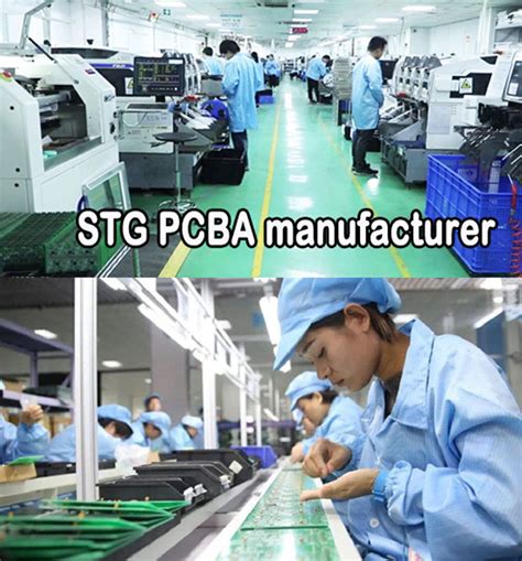
Once fabrication is complete, it’s time for PCB assembly (or PCBA), where components are placed and soldered onto the printed circuit board. Techniques like Surface Mount Technology (SMT) and Through-Hole Technology are widely used during this phase. Both methods offer distinct advantages in terms of space efficiency and ease of component integration. The assembly process culminates in testing to ensure functionality before final delivery. A well-executed PCB fabrication and assembly process ensures reliability and durability in various applications, making it imperative for manufacturers to adhere closely to established quality controls throughout these stages.
Techniques Used in PCB Assembly
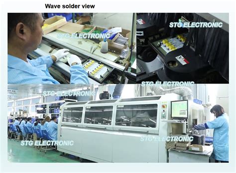
The techniques employed in PCB assembly (or PCBA) play a crucial role in ensuring the efficiency and reliability of electronic devices. One common method is surface mount technology (SMT), which involves placing electronic components directly onto the surface of a PCB. This technique allows for a more compact design, reducing the overall size of the circuit boards while enhancing performance. Another widely utilized approach is through-hole technology, where components are inserted into holes drilled into the PCB and soldered on the opposite side. This method is often favored for components that require strong mechanical support and reliability.
In addition to these methods, solder paste printing serves as an essential step in PCB assembly. During this process, solder paste is applied to designated areas on the PCB, facilitating better connection between components and their pads. The subsequent reflow soldering technique heats this paste to create solid electrical connections.
Moreover, automated optical inspection (AOI) is utilized post-assembly to identify defects or misalignments that may compromise the functionality of the board. This quality control measure ensures that every assembled unit adheres to strict standards before moving forward.
Understanding these PCB assembly techniques not only enhances project outcomes but also fosters innovation in electronic design—making it an essential area of focus for anyone involved in electronics manufacturing. As technology advances, these techniques are continually refined, paving the way for even greater efficiencies and capabilities in PCB assembly processes worldwide.

Materials for PCB Manufacturing
The selection of appropriate materials is crucial in the PCB fabrication and assembly process, as they directly influence the performance and reliability of the final product. The two primary components of any printed circuit board (PCB) are the substrate and the conductive material. The substrate, typically made of fiberglass, is responsible for providing structural integrity. Among the commonly used substrates are FR-4, a versatile glass-reinforced epoxy laminate, and CEM-1 and CEM-3, which offer different performance characteristics.
For conductive pathways, copper is the most widely used material due to its excellent conductivity and ductility. The thickness of copper layers in PCB designs can significantly affect electrical performance, making it essential to choose the right specifications for specific applications. Besides this, surface finishes are vital for enhancing solderability and preventing oxidation. Finishes like HASL (High-Quality Hot Air Solder Leveling), ENIG (Electroless Nickel Immersion Gold), and OSP (Organic Solderability Preservative) provide various benefits depending on assembly requirements.
In addition to these primary materials, other components such as solder masks and silkscreens also play crucial roles in PCB assembly (pcba). The solder mask protects conductive traces from accidental short circuits while enhancing aesthetics, whereas silkscreens provide identification markings that are essential during assembly.
Ensuring that all materials meet industry standards is vital; thus, quality control measures become indispensable in maintaining consistency throughout production. By carefully selecting materials tailored for specific functionalities during the pcb assembly process, manufacturers can streamline operations and enhance product reliability in complex electronic systems.
Quality Control Measures in PCB Production
In the world of PCB fabrication and assembly, quality control is paramount to ensure the reliability and functionality of the final product, commonly referred to as PCBA (Printed Circuit Board Assembly). Effective quality control measures encompass a variety of processes throughout the production cycle. Initially, incoming material inspection is critical; ensuring that all components meet the required specifications helps prevent downstream defects. Following this, rigorous testing procedures, such as Automated Optical Inspection (AOI), are implemented during both the manufacturing and assembly stages. This allows for early detection of potential issues, thereby reducing waste and rework.
Moreover, implementing a robust testing strategy, which may include functional testing and in-circuit testing, enhances the reliability of each PCBA produced. These tests ensure that each module functions correctly under expected conditions. Another essential aspect of quality control is maintaining comprehensive documentation throughout all stages to track performance metrics and problem areas, enabling continuous improvement.
Furthermore, employee training plays an instrumental role in quality assurance; skilled operators are less likely to make errors during assembly processes. Adoption of industry-standard quality assurance protocols, such as ISO 9001, reinforces a commitment to high-quality production. Ultimately, rigorous quality control measures not only improve product performance but also foster trust among customers in the reliability and durability of their electronic products.
Challenges in PCB Fabrication and Assembly
The world of PCB fabrication and assembly presents a variety of challenges that can significantly impact the efficiency and success of projects. One common issue is the complexity of designing PCBs that meet specific requirements while remaining manufacturable; this often leads to difficulties in the realization of custom designs. Additionally, maintaining high precision during the PCB assembly process is crucial, as deviations can result in malfunctioning products. The choice of materials also poses a challenge, as selecting the right substrates and components can influence both performance and cost. Furthermore, ensuring robust quality control measures is essential to address potential defects in both the fabrication and assembly phases. This need for rigorous testing can extend project timelines and necessitate additional resources. As technology advances, the rapid pace of innovation means that keeping up with new techniques and materials for PCBA becomes increasingly vital for manufacturers aiming to remain competitive. By recognizing these challenges upfront, stakeholders can streamline their processes, adopt best practices, and ultimately improve outcomes in their PCB fabrication and assembly projects.
Future Trends in PCB Technology
The landscape of PCB technology is evolving rapidly, driven by advancements that are reshaping pcb fabrication and pcb assembly processes. One significant trend is the rise of flexible PCBs, which provide greater design flexibility and enable the development of slimmer, lightweight devices. This adaptability supports emerging technologies like wearable electronics and IoT devices. Another key development is the integration of automated assembly techniques in the pcba process, which not only enhances speed but also improves consistency and reduces human error. Innovations in materials, such as high-frequency laminates and environmentally friendly substrates, are also gaining traction as they contribute to performance efficiency and sustainability. Additionally, as electronic components continue to shrink, microvias in PCB design are becoming more common, facilitating denser layouts while maintaining or improving connectivity. Companies that leverage these advancements in pcb assembly will not only enhance product quality but also gain a competitive edge in a market that demands innovation and reliability. By staying abreast of these trends, organizations can better position themselves for success in an increasingly technology-driven world.
Best Practices for Successful PCB Projects
To ensure the success of your PCB assembly projects, several best practices should be considered throughout the design and manufacturing processes. One essential aspect is to leverage meticulous design practices. Ensuring that your circuit board layout is optimized for manufacturability can significantly reduce errors during production. Incorporating clear and precise documentation, including schematics and diagrams, aids manufacturers in understanding your specifications and requirements. Furthermore, selecting high-quality materials is critical. Not only do they influence the durability and functionality of the final product, but materials that have been thoroughly vetted can reduce issues related to soldering during the PCBA process.
In addition, establishing robust communication channels with your manufacturer ensures that any potential issues or questions are quickly addressed. Engaging in early prototypes or test runs allows for immediate feedback, enabling engineers to iterate on designs before full-scale production begins. Regular quality control checks are also vital; implementing inspection techniques during both PCB fabrication and assembly stages maintains product integrity while minimizing defects.
Finally, staying updated on evolving technologies in PCB fabrication can provide competitive advantages. Emerging techniques such as automated PCBA processes can enhance efficiency and precision, leading to timely project completions under budget constraints. By adhering to these best practices, you can navigate the complexities of PCB projects more effectively while achieving optimal outcomes for your end products.
Conclusion
In summary, understanding PCB fabrication and assembly services is essential for anyone involved in electronics development. The intricacies of these processes, encompassing everything from design to final testing, play a pivotal role in the functionality of modern electronic devices. Each phase of pcb assembly, or PCBA, requires meticulous attention to detail and systematic quality control measures to ensure that the final product meets industry standards and performs reliably. Additionally, the choice of materials significantly impacts the durability and efficiency of the printed circuit boards (PCBs). As technology continues to advance, staying informed about emerging techniques and best practices is crucial for enhancing both productivity and innovation in PCB projects. Finally, by embracing these comprehensive processes, one can effectively streamline projects and tackle challenges that arise in hardware production. The dynamic nature of this industry demands a commitment to continuous learning and adaptation, which ultimately leads to successful outcomes in PCB fabrication and assembly.
FAQs
What is PCB assembly?
PCB assembly, commonly referred to as PCBA, is the process of connecting electronic components to a printed circuit board (PCB). This involves soldering the components onto the PCB to create a functional electronic device.
What are the types of PCB assembly processes?
The main types of PCB assembly processes include Surface Mount Technology (SMT) and Through-Hole Technology (THT). SMT is more widely used due to its efficiency and ability to accommodate smaller components.
What is the importance of quality control in PCB fabrication and assembly?
Quality control is crucial in PCB fabrication and assembly as it ensures that each board meets specific standards and specifications. This minimizes errors, enhances reliability, and reduces costs associated with defects or recalls.
How do I choose the right materials for my PCB project?
Choosing the right materials for your PCB project involves considering factors such as electrical conductivity, thermal resistance, flexibility, and intended application. Different materials can affect performance significantly.
What challenges are commonly faced during PCB fabrication?
Common challenges include issues with layer registration, material compatibility, soldering defects, and achieving proper surface finish. Addressing these challenges promptly can enhance overall production quality.
If you have further questions or need more detailed insights into PCB assembly, feel free to explore our services. For more information on quality processes and services related to PCBA, please click here: https://www.andwinpcb.com/pcb-assembly/