This article explains clearly what each layer of the Gerber file of the PCB board means
For novice electronic engineers, especially those who have never been exposed to PCB board making, when they hear the terms Gerber file, solder mask opening window, green oil and black oil, steel mesh opening, and exporting Gerber files to the board factory, they may be a little confused. Don’t be afraid. Below I will analyze the Gerber file, and the others will also be mentioned. After reading it, you will probably understand what is going on.
First use AI to answer what Gerber is: The Gerber file of PCB (Printed Circuit Board) is a standard file format used to describe the graphic information of each layer of PCB. The Gerber file is a key file for manufacturing PCBs. It contains all the necessary information so that PCB manufacturers can accurately produce the circuit boards expected by designers.
Let me speak human language and analyze an open source file as an example (everyone is welcome to communicate together. If there is anything inappropriate, please point it out in the comment area so that it can be corrected in time).
1.How to export Gerber files
Export after PCBLayout is completed and DRC is checked correctly.
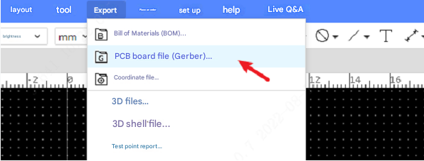
There are two options when exporting Gerber files:
One-click export: According to the default settings, all layers and primitives are exported, excluding drill tables and independent drill information files.
Custom configuration: Modify the configuration according to your own needs. Support drilling information and drill tables; support adding different configurations in the list on the left; support selecting exported layers; layer mirroring; support selecting exported primitive objects. When exporting, select a configuration for Gerber export.
Generally speaking, just export with one click. There is no need to worry about the functions in the custom configuration.
Other software also have Gerber export functions, so I won’t go into details here.
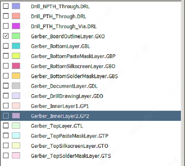
2.Gerber file analysis
I use Jiali Chuang DFM for analysis (you can also use other Gerber viewers or CAM tools to view and edit), analyze what each layer corresponds to, and which layer of the corresponding circuit board in the actual object.
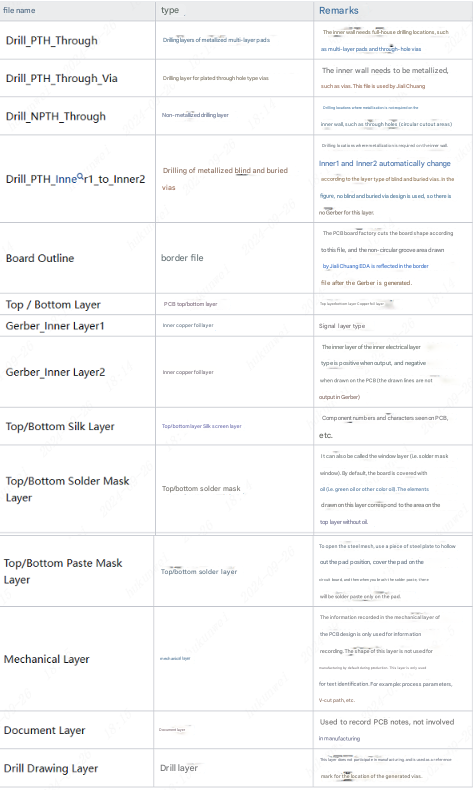
2.1. Layer table description
2.2. Perceptual analysis
The following is an analysis of the top silk screen layer, solder mask layer, soldering layer, and top copper foil layer to form an intuitive feeling.
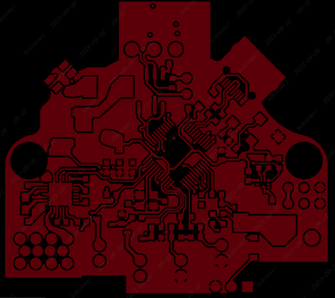
2.2.1. 2D simulation top layer:
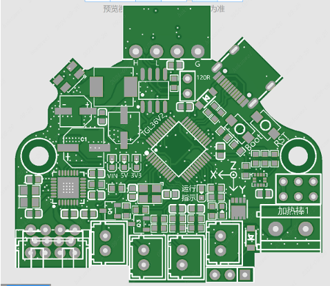
2.2.2. Top circuit layer
2.2.3. Top solder mask layer (the green ones)
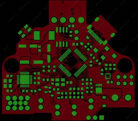
The solder mask layer can actually be called a window layer or a green oil layer. Its English name is solder mask. It refers to the place where green oil is to be laid on the PCB, and this solder mask layer uses negative film output, so after the shape of the solder mask layer is mapped to the board, it is not green oil solder mask, but the copper skin is exposed. When the copper skin is exposed, we are used to calling it a window.
That is, the green part of this picture will not be covered with ink, and the part without green will be covered with ink, which can also be seen by comparing it with the simulation picture.
2.2.4. Solder layer (also called solder paste layer) (the blue part):
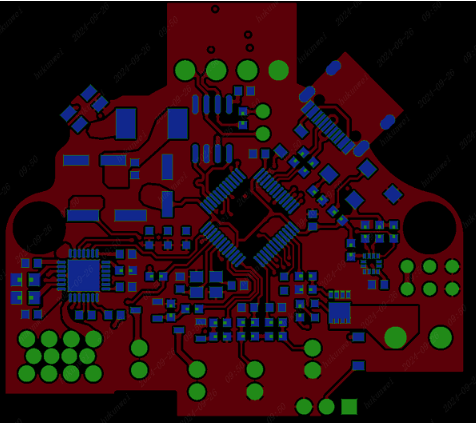
The blue part will be brushed with a layer of solder paste. At the same time, you can see that at the same pad position, the solder layer is slightly smaller than the solder mask layer.
2.2.5. Top silk screen layer
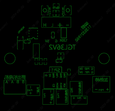
The yellow part is the silk screen layer.
Here we should mention the bottom silk screen layer. The Gerber file is shown in the figure below (Note: the bottom silk screen layer looks reversed when previewed, so it is positive when printed on the actual object (it is the same as the bottom device and silk screen are reversed when PCB layout is viewed). If the bottom silk screen is positive when previewed (actually it is not correct), it will be reversed when printed on the circuit board):
2.2.6. Summary
I will not show the via layer, inner layer, and bottom layer in pictures. You can open a Gerber file and analyze it yourself (you can export the Gerber file after drawing the PCB board yourself, or ask your predecessors for a copy. You can grow faster by standing on the shoulders of predecessors. Off topic, haha). After the Gerber analysis, you can directly make the board. If it is a batch, it is recommended to conduct a manufacturability analysis.
3.The difference between different board layers Gerber
For Gerber files, the Gerber of high-layer PCB boards will have more inner layer files than the Gerber of single-layer and double-layer PCB boards.
Finally, let’s briefly talk about the difference between 1-layer, 2-layer, 4-layer, 6-layer, 8-layer and other circuit boards.
First, the number of layers of high-layer PCBs is usually more than 4 layers, and can even reach 20 layers or more.
These additional layers allow for higher wiring density and more complex circuit design, which is suitable for scenarios requiring high-speed signal transmission and high-frequency applications. In contrast, single-layer and double-layer PCBs have lower wiring density and are suitable for simple circuits and low-speed signal transmission.
Secondly, the electrical performance of high-layer PCBs is excellent.
The multi-layer structure can optimize the design of power and ground planes, reduce signal interference and electromagnetic compatibility (EMC) issues, and ensure signal integrity. Single-layer and double-layer PCBs have limited capabilities in this regard and are generally not suitable for high-performance and high-reliability applications. (In terms of reducing parasitic inductance and reducing wiring space, I like to use JLC’s 6-layer board via-in-disk process. This process not only improves the performance of my circuit board, but also does not increase the price. If you have other new processes now, you can also propose them. Everyone can learn about them).
In terms of thermal management, high-layer PCBs also have advantages.
The multi-layer structure can optimize the heat dissipation path through the inner layer design, improve the heat dissipation efficiency, and is suitable for high-power and high-heat applications. The thermal management capabilities of single-layer and double-layer PCBs are weak, and usually can only be met by simple heat dissipation design.
In terms of manufacturing process, the manufacturing process of high-layer PCBs is more complicated, requiring the use of advanced technologies such as lamination, blind buried vias, and via-in-disk, and the manufacturing cost is high. The manufacturing process of single-layer and double-layer PCBs is relatively simple, the cost is low, and it is suitable for mass production and fast delivery. In summary, high-layer PCBs are different from single-layer and double-layer PCBs in terms of number of layers, wiring density, electrical performance, thermal management, and manufacturing process. High-layer PCBs are suitable for complex and small-area applications, while single-layer and double-layer PCBs are suitable for applications that require cost compression.
4.Final chat
Now in the market, many people say that PCB layout is the work of a wire puller. I disagree. In fact, I want to say that taking a four-layer or six-layer board and adding power and ground layers without thinking, and then connecting the wires, this is indeed a wire puller (please don’t criticize me). But if you need to consider signal integrity, power integrity, electromagnetic compatibility, power-on timing, etc. on a high-layer board. Or at the request of the boss, you want to reduce costs, space and number of layers (especially consumer electronics), then use single-layer boards and double-layer boards. These actually have very high requirements for layout and wiring, and the technical content is not bad. Is the person responsible for PCB layout in your company a wire puller or a stable product implementer?