Live PCB Design and Manufacturing Techniques Unveiled
Key Takeaways
In the realm of PCB assembly and manufacturing, understanding the intricate evolution of design and technique is paramount. Recent advancements have showcased how the integration of smart technologies and innovative methodologies are reshaping the landscape. For instance, embracing multilayer designs can significantly enhance functionality while maintaining space efficiency. Essential tools such as advanced CAD software play a pivotal role in this transformation, allowing designers to create precise layouts that streamline the overall production process.
Moreover, common challenges in PCB design can often stem from overlooked details—something that experienced professionals advise against. “Always double-check your connections and component placements to minimize errors during assembly,” is sage advice from industry experts emphasizing the importance of meticulousness in each project.
As you dive deeper into advanced techniques such as surface mount technology, remember to incorporate effective quality control measures to ensure reliability and performance of your designs. The evolving landscape also beckons attention to future trends; being proactive about emerging technologies will greatly enhance your skills and project outcomes in pcba endeavors.
“Stay curious and continually explore new tools and methodologies; innovation is key to success.”
The Evolution of PCB Design: Trends and Innovations
The field of PCB design has undergone significant transformations over the years, driven by advancements in technology and the growing demands of various industries. One notable evolution is the shift toward more compact and efficient PCB assembly techniques, which allow for the creation of smaller, more powerful electronic devices. This trend underscores the importance of thorough knowledge in PCBA processes to ensure that designs are both functional and manufacturable.
Furthermore, modern design trends increasingly emphasize sustainability, leading to innovations such as eco-friendly materials and manufacturing processes that reduce waste. The integration of automated tools has also become prevalent in contemporary PCB design workflows, enhancing precision and reducing lead times in production.
To illustrate these trends, here’s a brief overview of current innovative techniques employed in PCB design:
| Technique | Description |
|---|---|
| Multi-layer PCBs | Enhances circuit density by stacking layers |
| Flexible PCBs | Allows for bending and fitting in compact spaces |
| 3D Printing | Facilitates rapid prototyping and customization |
| High-Frequency Designs | Optimizes performance for fast signal transmission |
As we look forward to future developments, it is essential to stay informed about these trends that not only influence how designs are created but also define how they fit into larger manufacturing systems to meet growing market demands. By understanding these innovations, designers can effectively enhance their skill set and elevate their projects to new levels of success.
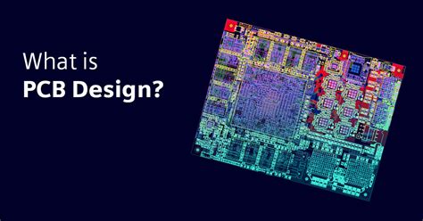
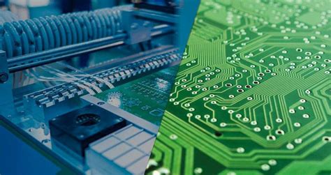
Essential Tools and Software for Modern PCB Manufacturing
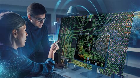
In the fast-paced world of electronics, having the right tools and software for PCB design is essential for anyone looking to excel in pcb assembly and production. The market has seen a rise in sophisticated software solutions that cater to various needs, from schematic capture to layout design. Leading software programs such as Altium Designer, Eagle, and KiCAD provide users with intuitive interfaces and powerful features that facilitate efficient design workflows. These tools enable designers to visualize their circuits, simulate performance, and identify potential issues before moving on to the physical pcba process. Moreover, integrating modern CAD software into the workflow not only streamlines the design process but also enhances collaboration among team members. As technology continues to advance, tools that incorporate features like automated routing and multi-layer support further empower designers to tackle complex projects with confidence. Additionally, selecting the proper fabrication software is crucial when transitioning from design to manufacturing; this ensures that communication with fabrication houses remains smooth and accurate. Embracing these essential technologies will undoubtedly help professionals take their PCB projects from concept to reality with improved precision and efficiency.
Step-by-Step Guide to Creating Efficient PCB Layouts
Creating an efficient PCB layout is essential for achieving optimal performance in electronic projects. To begin, understanding the fundamentals of PCB design is crucial. This involves having a clear outline of the intended purpose of your PCBA (Printed Circuit Board Assembly), as it guides the layout process. Start with selecting the appropriate components and ensuring they are properly placed to minimize noise and interference. The arrangement should favor a logical flow of signals, allowing for shorter traces and maximizing efficiency.
Next, leverage advanced tools and software to simulate circuit behavior before finalizing your layout. These tools provide valuable insights by identifying potential issues related to electromagnetic interference or thermal management early in the design phase. As you create your layout, adhere to design rules that optimize space while preventing trace crowding and ensuring adequate grounding.
When laying out power and ground planes, use wider traces for high-current paths and confirm that there are multiple vias for grounding to ensure stability throughout the PCBA process. Finally, thoroughly review your designs using error-checking features offered by most design software; this step is paramount in preventing costly reworks during manufacturing.
By following these guidelines, you can enhance not only the efficiency of your PCB layouts, but also the reliability of your final product, paving the way for successful PCB assembly outcomes.
Expert Insights: Overcoming Common PCB Design Challenges
In today’s fast-paced technology landscape, PCB design is essential for a wide range of electronic applications. However, designers often face significant challenges that can hinder the overall effectiveness of their projects. One common issue is maintaining the balance between performance and cost-efficiency. Designers need to ensure that the PCB assembly processes do not escalate expenses without compromising on quality. Furthermore, managing pcba (Printed Circuit Board Assembly) complexity becomes crucial as device sizes shrink and functionalities expand. Advanced routing techniques and careful component placement can help in optimizing the layout and enhancing manufacturability.
Another challenge involves thermal management, as components generate heat that can affect operation. Proper heat dissipation methods should be considered from the outset, integrating features such as thermal vias or selecting materials with good thermal properties to aid in cooling. Additionally, ensuring compatibility with manufacturing processes is vital; including design rules that cater to fabrication techniques can significantly reduce the risk of errors during PCB manufacturing.
Collaboration with manufacturing teams early in the design phase has proven beneficial in overcoming common obstacles associated with poor designs leading to assembly difficulties. By integrating feedback from both designers and engineers, a smoother transition from design to production can be achieved, ultimately fostering a more efficient pcba process.
Addressing these challenges not only improves individual projects but also enhances overall productivity and operational success in PCB design endeavors.
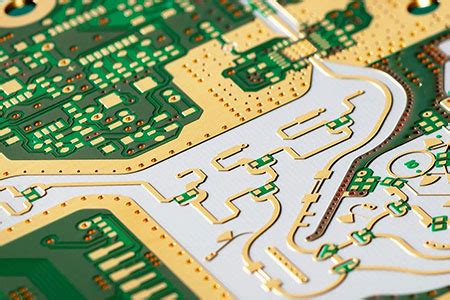
Advanced Techniques in PCB Fabrication and Assembly
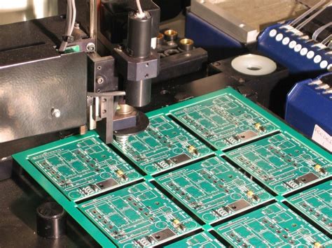
In today’s competitive landscape, the advancements in PCB fabrication and assembly processes are crucial for enhancing the performance and reliability of electronic devices. One cutting-edge technique involves the integration of automated assembly lines, which significantly improve efficiency and reduce human error during the PCBA process. By utilizing sophisticated robots and AI-driven technology, manufacturers can achieve higher precision in component placement, thereby optimizing overall yield rates.
Another notable innovation is the application of advanced materials, such as flexible substrates and high-density interconnects (HDI), which allow for more compact designs without compromising functionality. This enables engineers to push the boundaries of traditional designs, leading to smaller and lighter devices that cater to modern consumer preferences. Moreover, implementing surface mount technology (SMT) has transformed how components are soldered onto PCBs, enhancing durability and performance in various operational environments.
Quality assurance remains a key focus in modern PCB assembly; thus, incorporating stringent testing protocols is vital. Techniques such as automated optical inspection (AOI) and X-ray inspection are increasingly employed to detect faults early in the production process. This proactive approach not only ensures that any defective PCBA units can be identified swiftly but also enhances customer satisfaction by delivering superior products.
As the industry continues to evolve, embracing these advanced techniques will empower designers and manufacturers to create innovative solutions that meet diverse market demands while reinforcing their competitive edge. By staying abreast of these developments, professionals can refine their skills and elevate their projects to new heights of excellence.
Quality Control Measures in PCB Production
In the realm of PCB production, ensuring the highest standards of quality is paramount. Quality control measures play a crucial role in not only assessing the integrity of printed circuit boards but also in ensuring successful PCB assembly (PCBA). Various strategies can be employed, including rigorous inspection processes throughout all stages of production. This may involve the use of automated optical inspection (AOI) systems to detect defects early on, thus minimizing costly rework and ensuring that the final product meets industry standards. Additionally, implementing statistical process control (SPC) helps monitor quality metrics and identify any variations that could affect performance or reliability. It is equally essential to conduct functional testing, where assembled boards undergo checks to ensure they perform according to specifications. Adopting a multifaceted approach toward quality control not only enhances product reliability but also builds trust with clients and end-users, ultimately contributing to the advancement of PCBA techniques and outcomes in today’s evolving marketplace.
Future Trends in PCB Technology to Watch Out For
As the landscape of PCB design and manufacturing continues to evolve, several trends are emerging that signify the future direction of printed circuit board (PCB) technology. One such trend is the increasing adoption of flexible PCBs, which allow for lighter, more compact devices, enabling engineers to push the boundaries of design in consumer electronics and other applications. Coupled with this, advancements in pcb assembly techniques such as robotic assembly and automated testing are shaping a more efficient manufacturing process. The integration of IoT functionalities into PCBs is also gaining traction, paving the way for smart devices that communicate effortlessly with one another. Additionally, as sustainability takes center stage in manufacturing practices, the shift towards eco-friendly materials for both PCB fabrication and assembly processes is notable. Emerging technologies like 3D printing are also making their mark, leading to rapid prototyping capabilities and innovative designs. Keeping abreast of these trends will not only enhance your ability in crafting effective PCBs but also ensure your projects stand out in an increasingly competitive marketplace where pcba remains a key focus.
Enhancing Your Skills: Practical Tips for Better PCB Projects
To elevate your PCB projects, it is essential to incorporate sound design principles and practical techniques that can significantly enhance the performance and reliability of your PCB assembly processes. Start by thoroughly understanding the fundamentals of PCBA and the role that each component plays in the overall functionality. Utilizing advanced software tools can streamline your design workflow, enabling you to create intricate layouts efficiently. Pay close attention to trace width, spacing, and layer stacking; these factors directly impact the electrical performance of your board.
Additionally, don’t overlook the importance of simulation software. It allows you to test your designs under various conditions before physical production, which minimizes errors and reduces costs. In terms of materials, selecting high-quality substrates can improve thermal management and signal integrity, particularly in high-frequency applications. Remember to incorporate proper grounding techniques and consider EMI shielding if your project deals with sensitive signals.
Finally, learning from industry experts through workshops, webinars, or community forums can provide valuable insights into overcoming common challenges faced during PCB assembly. Engaging with peers can also spark creative solutions that may enhance your designs while keeping you abreast of emerging trends in PCB manufacturing technology. By combining these practical tips with continuous learning, you will undoubtedly see improvements in the quality and efficiency of your PCB projects.
Conclusion
In today’s rapidly advancing electronics landscape, the significance of effective PCB assembly techniques cannot be overstated. As we have explored throughout this session, the evolution of PCB design and manufacturing has brought forth a myriad of innovative tools and methodologies. From traditional methods to cutting-edge advancements in pcba, each phase of the process offers opportunities to enhance quality and efficiency. The integration of modern software into PCB manufacturing not only streamlines workflows but also empowers designers to create more complex and reliable layouts. Furthermore, adopting best practices in quality control ensures that each assembled board meets stringent industry standards, fostering trust in the finished product. As we continue to witness transformations in PCB technology, staying informed about future trends will be crucial for anyone looking to elevate their projects. Engaging with expert insights and techniques shared in our session can significantly improve your grasp on pcb assembly, making you better equipped to tackle design challenges head-on and innovate within your own projects.
FAQs
What is PCB assembly?
PCB assembly, or PCBA, is the process of soldering electronic components onto a printed circuit board, allowing it to function as designed. This crucial step in electronics manufacturing integrates both the design and the fabrication phases.
What are the main techniques used in PCB assembly?
There are various techniques employed in PCB assembly, including surface mount technology (SMT) and through-hole mounting. Each method has its own advantages depending on factors like component size, board complexity, and manufacturing volume.
How can I improve my PCB design skills?
To enhance your PCB design skills, it’s essential to stay updated with the latest trends in technology, utilize advanced tools suited for your needs, and engage with communities that discuss challenges and share solutions related to pcba.
What quality control measures should I implement in PCB production?
Implementing thorough quality control measures involves regular inspections at various stages of production, utilizing automated optical inspection (AOI) systems, and conducting electrical testing to ensure faultless operation of the assembled PCBs.
What are some challenges faced during PCB manufacturing?
Common challenges include managing design complexity, ensuring signal integrity, and maintaining efficiency during the assembly process. Addressing these issues can lead to improved product performance and reduced manufacturing costs.