Understanding Fine Pitch PCB Assembly Techniques and Benefits
Key Takeaways
Fine pitch PCB assembly is a pivotal component in the evolution of modern electronics. As devices become increasingly compact, the demand for PCB assembly techniques that support high-density circuit designs grows. Notably, the agility to work with fine pitch technology offers significant advancements in both performance and reliability. The benefits of utilizing fine pitch PCBs include enhanced performance through optimized layouts that minimize signal interference and greater efficiency in space utilization. However, this technology comes with notable challenges such as a heightened risk of manufacturing defects if proper techniques are not engaged during the assembly process.
To address these complexities, employing best practices is essential for achieving efficient PCBA. Adopting advanced tools and equipment contributes to better handling and accuracy during assembly, reducing potential errors associated with manual processes. As manufacturers gain experience with fine pitch technology, they develop greater proficiency in mitigating common issues like solder bridging and misalignment. These challenges emphasize the need for continuous improvement and innovation within the domain of PCB assembly.
| Aspect | Importance |
|---|---|
| High-Density Structures | Facilitates compact design |
| Soldering Techniques | Ensures reliability for microjoint connections |
| Equipment Used | Directly impacts workflow efficiency |
| Common Defects | Understanding ways to mitigate issues |
Overall, the strategic application of fine pitch PCB assembly techniques not only enhances product performance but also streamlines production processes, underpinning significant advancements within electronic manufacturing sectors. The continuous evolution in this area will be critical as the technology landscape shifts towards increasingly sophisticated electronic devices.
Introduction to Fine Pitch PCB Assembly
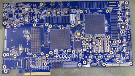
Fine pitch PCB assembly refers to the intricate process of assembling printed circuit boards (PCBs) with smaller component leads and tighter spacing compared to the traditional design. As electronic devices become smaller, lighter, and more powerful, the demand for fine pitch technology has increased significantly. This assembly technique enables engineers to fit more components into a given area, which is essential for modern consumer electronics, telecommunications, and automotive applications. The ability to utilize finer pitches not only enhances functionality but also boosts the overall efficiency of the devices.
"Incorporating fine pitch PCB assembly into your design can lead to significant improvements in both performance and reliability."
However, it is crucial to address that while fine pitch designs offer these advantages, they also present unique challenges, such as alignment precision during soldering and potential issues with heat dissipation. Attention to detail in the assembly process, using high-quality tools and adhering to best practices can mitigate such challenges, ensuring that the final product operates optimally. With advancements in technology and PCB manufacturing processes, achieving a successful PCBA with fine pitch components has never been more feasible.
Key Techniques in Fine Pitch PCB Assembly
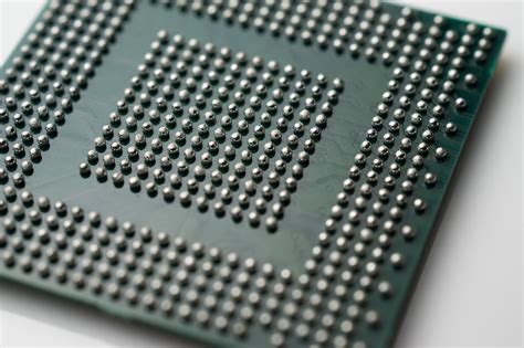
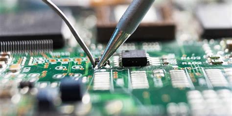
Fine pitch PCB assembly has garnered significant attention due to its pivotal role in advancing electronic device capabilities. One of the key techniques utilized in this area is the use of advanced solder paste printing methods, which require precision alignment to ensure optimal functionality. The application of high-resolution screen printing or stencil printing helps achieve uniform solder paste distribution, crucial for maintaining connections between closely spaced pads.
Additionally, pick and place technology has evolved to support the placement of components on fine pitch layouts. With automated systems equipped with vision inspection, these machines can identify and correct placement errors, enhancing the reliability of the final PCBA. Another vital technique is reflow soldering, which must be carefully calibrated to accommodate the delicate nature of fine pitch components, preventing thermal stress that could lead to damage.
Thermal profiling during reflow is essential too, as ensuring even heating contributes to strong solder joints. Moreover, employing advanced inspection methods, such as automated optical inspection (AOI), ensures that any defects are identified early on in the assembly process. These sophisticated techniques not only enhance efficiency but also contribute significantly to the reliability and performance of modern electronic devices made possible by fine pitch technology.
Benefits of Fine Pitch Technology in Modern Electronics
The incorporation of fine pitch PCB assembly techniques has brought about transformative benefits for modern electronics, particularly in the realm of high-density circuit designs. One of the foremost advantages is the ability to achieve higher component density, which facilitates the miniaturization of electronic devices without compromising functionality. This is crucial in an era where consumer demand leans towards smaller, more powerful gadgets. Further, fine pitch technology enhances signal integrity, reducing the risks of interference and ensuring that signals maintain clarity over longer distances. Additionally, by utilizing smaller components with narrower pitches, manufacturers can create circuits that consume less power, contributing to energy-efficient designs.
Moreover, the ability to integrate advanced features within a compact space paves the way for innovations such as sophisticated wearables and intricate medical devices that rely heavily on PCB assembly for their operation. The emphasis on reliability is equally important; fine pitch techniques promote robust connections that can withstand various environmental factors, which is a significant consideration in industries like automotive and aerospace where durability is paramount. In summary, adopting fine pitch technology not only streamlines the design process but also leads to enhanced performance and longevity in electronic products, substantiating its pivotal role in advancing modern electronics.
Common Challenges in Fine Pitch PCB Assembly
The process of fine pitch PCB assembly presents several obstacles that can impact the overall efficiency and reliability of the final product. One major challenge is the precise alignment of components on the PCB. As designs become more intricate and PCBA features narrower spacing, any misalignment can hinder functionality and increase rejection rates. Moreover, soldering techniques must adapt to accommodate the smaller pitch sizes; traditional methods may not deliver sufficient reliability, raising concerns over joint integrity as well as potential cold solder joints.
Cleaning processes for these assemblies are also more complicated due to the dense layout, where contaminants may become trapped in tight spaces, leading to long-term reliability concerns. Additionally, handling delicate components poses a risk of mechanical damage. The increased risk of solder bridging during assembly further complicates the process and necessitates skilled operators alongside advanced equipment for effective management.
In summary, while fine pitch technology opens new avenues in electronic design, it also requires careful consideration of challenges such as component alignment, soldering techniques, contamination management, and potential damage during handling. Addressing these challenges with precise techniques and tools is crucial to enhancing both productivity and the overall success of PCB assembly in high-density applications.
Best Practices for High-Density Circuit Design
When approaching high-density circuit design, it is crucial to implement best practices that enhance the efficiency and reliability of PCB assembly. One essential practice is to ensure optimal component placement; this minimizes the distance between connections and can significantly reduce signal loss and interference. Additionally, employing fine pitch PCB assembly methods necessitates precise manufacturing tolerances. It is recommended to utilize advanced soldering techniques, such as reflow soldering or selective soldering, which are specifically designed to accommodate the intricate nature of fine pitch components. Furthermore, utilizing automated processes like pick-and-place can enhance consistency during assembly—ensuring that components are accurately positioned on the PCBA.
An integral aspect of high-density design is thorough thermal management; as component density increases, so does the heat generated during operation. Using thermal vias and adequate heatsinking techniques ensures efficient heat dissipation, maintaining component integrity over time. Implementing robust testing procedures throughout the assembly process will also help identify potential defects early on, which is critical for maintaining quality control in high-density circuits. As designs become increasingly complex, collaboration with skilled engineers familiar with fine pitch technology becomes essential to tackle challenges related to miniaturization while ensuring optimal performance in electronic applications.
Tools and Equipment for Efficient Assembly
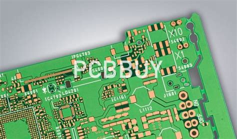
In the realm of fine pitch PCB assembly, having the right tools and equipment is essential to ensure precision and quality. Assemblies that utilize fine pitch technology often demand highly specialized PCB assembly tools capable of handling smaller components with intricate configurations. For instance, pick-and-place machines are vital, as they accurately position components on a circuit board, minimizing the risk of misalignment. Additionally, using advanced soldering techniques, such as reflow soldering, guarantees a reliable connection that can withstand the intricate demands of high-density designs.
A noteworthy consideration is the implementation of automated optical inspection (AOI) systems which play a pivotal role in enhancing the efficiency of the PCBA process. These systems provide real-time feedback on component placement and solder joint integrity, allowing for immediate corrections before proceeding to later assembly stages. Moreover, integrating stencils made from materials like stainless steel ensures even solder application across multiple pads, crucial for achieving uniformity in dense layouts.
To optimize workflows further, utilizing ergonomic tools can significantly reduce operator fatigue during manual assembly tasks. Tools designed with user comfort in mind allow technicians to maintain focus and precision throughout prolonged operations. Coupled with robust training programs that familiarize operators with both equipment use and best practices in fine pitch techniques, manufacturers can elevate their assembly processes to meet modern electronic requirements efficiently.
Case Studies: Successful Applications of Fine Pitch PCBs
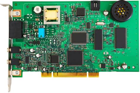
The effectiveness of fine pitch PCB assembly (also known as PCBA) becomes evident when examining real-world applications across various industries. In the telecommunications sector, companies have leveraged fine pitch technology to develop compact devices that require dense interconnections while maintaining high performance. One notable case involved the production of a state-of-the-art mobile communication device where the integration of fine pitch components reduced board space by nearly 30%, allowing for a sleeker design and improved functionality.
In the realm of medical devices, a manufacturer utilized fine pitch PCBs in portable health monitoring equipment. By utilizing innovative assembly techniques, they successfully reduced the size of their devices without compromising on crucial performance metrics. The meticulous process involved in their pcb assembly ensured reliability and efficiency, which are vital in healthcare applications. The results demonstrated that enhancing signal integrity and minimizing signal loss were achievable through advanced assembly methods which catered to the unique demands of their products.
Furthermore, in automotive electronics, the implementation of fine pitch PCB technologies facilitated more efficient energy management systems. One manufacturer achieved remarkable improvements in both durability and efficiency by integrating densely packed components that enabled enhanced functionality within limited space constraints. This demonstrates how successful applications can drive innovation and spur further advancements in diverse fields through effective use of PCBA processes.
These case studies highlight not only the versatility of fine pitch PCB assembly, but also its critical role in shaping future technology trends, providing insights into achieving reliable and efficient designs for high-density circuits across multiple sectors.
Future Trends in PCB Technology and Assembly Techniques
As the electronics industry continues to evolve, the landscape of PCB assembly is experiencing significant transformation driven by advancements in technology. The quest for more compact and efficient designs is steering a shift towards fine pitch PCB assembly, which facilitates the integration of smaller components into high-density layouts. Recent developments in materials and techniques are enabling manufacturers to achieve greater precision and reliability in their PCBA processes. Moreover, the rise of automation and the incorporation of artificial intelligence are poised to enhance operational efficiency, enabling faster turnaround times while minimizing human error. The ongoing push for miniaturization will further foster innovation in fine pitch techniques, whereby optimized soldering processes, such as selective soldering and advanced reflow methods, are becoming increasingly prevalent. It is essential for professionals in the field to stay attuned to these trends as they will dictate not only the standards for quality and performance but also influence cost strategies within the competitive market landscape. As we look ahead, the emphasis on sustainability is also becoming a crucial factor in PCB assembly, prompting a reevaluation of materials and practices that prioritize environmental impact alongside performance metrics. This multi-faceted evolution signifies an exciting era within PCB technology that promises to reshape how electronic devices are developed and manufactured.
Conclusion
In summary, the advancement of fine pitch PCB assembly has revolutionized the electronics industry by enabling the creation of high-density circuit designs that were previously unattainable. The pcba process not only optimizes space but also enhances the performance of electronic devices, catering to the growing demand for compact yet powerful technology. However, this innovation does come with its set of challenges, such as handling smaller components and ensuring proper alignment during assembly. Adhering to best practices in fine pitch PCB assembly is crucial for maximizing efficiency and reliability. By employing the right tools and equipment, as discussed in previous sections, manufacturers can achieve outstanding results and pave the way for future trends in PCB technology. Understanding these dynamics not only benefits manufacturers but also serves end-users who rely on high-performance electronics in their daily lives. As the industry evolves, continuous improvement in pcb assembly techniques will remain pivotal in shaping technological advancements.
FAQs
What is fine pitch PCB assembly?
Fine pitch PCB assembly refers to the process of assembling printed circuit boards (PCBs) with components placed closely together, often requiring specialized techniques and equipment due to the reduced spacing between pins or pads.
What are the key challenges associated with fine pitch PCBA?
The primary challenges include difficulties in soldering and alignment, potential for bridging, and the need for advanced inspection technologies to ensure reliability and performance of the assembled boards.
What benefits does fine pitch technology offer in modern electronics?
The benefits of fine pitch technology include improved space efficiency, allowing for smaller devices, enhanced performance due to shorter signal paths, and increased component density that meets the demands of contemporary electronic applications.
What tools are necessary for efficient assembly of fine pitch PCBs?
Necessary tools include precision soldering equipment, automated pick-and-place machines, reflow ovens, and inspection systems like X-ray or automated optical inspection (AOI) machines to ensure quality control throughout the PCB assembly process.
How can companies overcome challenges in fine pitch PCB assembly?
Companies can implement best practices such as thorough design reviews, using high-quality materials, investing in advanced machinery, conducting regular training for operators, and adopting stringent testing protocols to mitigate common challenges.