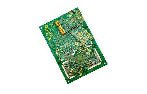
Precautions in PCB design
As an electronic engineer, designing circuits is a necessary hard work. However, no matter how perfect the principle design is, if the circuit board design is unreasonable, the performance will be greatly reduced, and in serious cases, it may not work properly. Based on my experience, I have summarized the following points that should be paid attention to in PCB design, hoping to be inspiring to you.
No matter what software is used, PCB design has a general procedure. It will save time and effort to follow the order, so I will introduce it according to the production process. (Because the interface style of Protel is close to Windows, the operating habits are also similar, and it has powerful simulation functions, it is used by many people, and this software will be used as an example.)
Schematic design is the preliminary preparation work. It is often seen that beginners directly draw PCB boards to save trouble, which will not be worth the loss. For simple boards, if you are familiar with the process, you may as well skip it. However, for beginners, you must follow the process. On the one hand, this can develop good habits, and on the other hand, it is the only way to avoid mistakes for complex circuits.
When drawing schematics, pay attention to the fact that each file should be connected as a whole in the hierarchical design, which is also of great significance for future work. Due to the difference in software, some software may appear to be connected but not actually connected (in terms of electrical performance). If you do not use relevant detection tools to detect, if there is a problem, it will be too late to find it after the board is made. Therefore, the importance of doing it in order is repeatedly emphasized, hoping to attract everyone’s attention.
The schematic diagram is based on the designed project. As long as the electrical connection is correct, there is nothing to say. Let’s focus on the specific problems in the board making process.
1.Make a physical border
The closed physical border is a basic platform for the future component layout and routing, and it also constrains the automatic layout. Otherwise, the components from the schematic diagram will be at a loss. But you must pay attention to accuracy here, otherwise it will be a big trouble if there are installation problems in the future. In addition, it is best to use arcs at the corners. On the one hand, it can avoid sharp corners from scratching workers, and at the same time it can reduce stress. In the past, one of my products always had a case of broken PCB board on the shell of some machines during transportation. It was fine after using arcs.
2.Introduction of components and networks
It should be simple to introduce components and networks into the drawn borders, but problems often occur here. You must carefully solve the errors one by one according to the prompts, otherwise it will take more effort later. The problems here are generally the following:
The packaging form of the component cannot be found, there are problems with the component network, and there are unused components or pins. These problems can be solved quickly by referring to the prompts.
3.Component layout
The layout and routing of components have a great impact on the life, stability, and electromagnetic compatibility of the product, and they should be paid special attention to. Generally speaking, there should be the following principles:
3.1 Placement order
First place the components related to the structure in fixed positions, such as power sockets, indicator lights, switches, connectors, etc. After these components are placed, use the LOCK function of the software to lock them so that they will not be moved by mistake in the future. Then place special components and large components on the circuit, such as heating components, transformers, ICs, etc. Finally, place small components.
3.2 Pay attention to heat dissipation
Pay special attention to heat dissipation when arranging components. For high-power circuits, heat-generating components such as power tubes and transformers should be placed as close to the side as possible to facilitate heat dissipation. They should not be concentrated in one place, and high capacitors should not be too close to avoid premature aging of the electrolyte.
4.Wiring
Wiring principles
The knowledge of wiring is very profound, and everyone will have their own experience, but there are still some common principles.
◆High-frequency digital circuits should be thinner and shorter
◆Attention should be paid to the isolation between high-current signals, high-voltage signals and small signals (the isolation distance is related to the withstand voltage. Usually, the distance on the board is 2mm at 2KV, and it should be increased in proportion above this. For example, if it is to withstand a 3KV withstand voltage test, the distance between the high and low voltage lines should be more than 3.5mm. In many cases, grooves are opened between the high and low voltage on the printed circuit board to avoid creepage.)
◆When wiring two panels, the wires on both sides should be perpendicular, oblique, or curved to avoid parallelism to reduce parasitic coupling; printed wires used as input and output of the circuit should be avoided as much as possible to avoid adjacent parallelism to avoid feedback. It is best to add a ground wire between these wires.
◆The corner of the routing should be greater than 90 degrees as much as possible, and the corners below 90 degrees should be eliminated, and 90-degree corners should be used as little as possible
◆For the same address line or data line, the routing length difference should not be too large, otherwise the short part of the line needs to be compensated by artificial bending
◆Try to route the wiring on the welding surface, especially for PCBs with through-hole technology
◆Try to use vias and jumpers as little as possible
◆The pads of the single-sided board must be large, and the wires connected to the pads must be thick. If teardrops can be placed, teardrops should be placed. The quality of general single-sided board manufacturers is not very good, otherwise there will be problems with welding and re-work
◆Large-area copper plating should be grid-shaped, so as to Prevent bubbles from forming on the board during wave soldering and bending due to thermal stress. However, in special occasions, the direction and size of GND should be considered. It cannot be simply filled with copper foil, but it needs to be routed.
◆ Components and routing cannot be placed too close to the edge. Generally, single-sided boards are mostly paper boards, which are easy to break after being stressed. If the wiring or components are placed on the edge, it will be affected.
◆ The convenience of production, debugging, and maintenance must be considered.
For analog circuits, it is very important to deal with the ground problem. The noise generated on the ground is often inconvenient to predict, but once it occurs, it will bring great trouble. You should prepare for it. For power amplifier circuits, extremely small ground noise will have a significant impact on the sound quality due to the amplification of the back stage; in high-precision A/D conversion circuits, if there is a high-frequency component on the ground line, it will produce a certain temperature drift, affecting the operation of the amplifier. At this time, you can add decoupling capacitors to the 4 corners of the board, one leg connected to the ground on the board, and one leg connected to the mounting hole (connected to the housing through screws). In this way, this component can be taken into account, and the amplifier and AD will be stable.
In addition, electromagnetic compatibility issues are even more important as people are paying more attention to environmentally friendly products. Generally speaking, there are three sources of electromagnetic signals: signal source, radiation, and transmission line. Crystal oscillator is a common high-frequency signal source. The energy value of each harmonic of the crystal oscillator in the power spectrum will be significantly higher than the average value. A feasible approach is to control the amplitude of the signal, ground the crystal oscillator shell, shield the interference signal, and use special filtering circuits and devices.
It should be noted that the serpentine routing has different functions in different applications. It is used in some clock signals in the computer motherboard, such as PCIClk and AGP-Clk. It has two functions: 1. Impedance matching 2. Filter inductance.
For some important signals, such as HUBLink in the INTELHUB architecture, there are a total of 13, with a frequency of up to 233MHz, and they must be strictly equal in length to eliminate the hidden dangers caused by time lag. At this time, serpentine routing is the only solution.
Generally speaking, the line spacing of the serpentine routing is ≥= 2 times the line width; if it is in an ordinary PCB board, in addition to the role of filtering inductance, it can also be used as an inductor coil for a radio antenna, etc.
5.Adjustment and improvement
After completing the wiring, what needs to be done is to make some adjustments to the text, individual components, and routing, as well as copper plating (this work should not be done too early, otherwise it will affect the speed and cause trouble for the wiring), which is also for the convenience of production, debugging, and maintenance.
Copper plating usually refers to filling the blank area left after wiring with a large area of copper foil.
You can lay GND copper foil or VCC copper foil (but in this way, if a short circuit occurs, it is easy to burn the device, so it is best to ground it, unless it is used to increase the conduction area of the power supply to withstand a larger current before connecting VCC). Grounding usually refers to using two ground wires (TRAC) to wrap a bunch of signal wires with special requirements to prevent it from being interfered with or interfering with others.
If you use copper plating instead of grounding wires, you must pay attention to whether the entire ground is connected, the current size, flow direction, and whether there are special requirements to ensure that unnecessary mistakes are reduced.
6.Check and verify the network
Sometimes due to misoperation or negligence, the network relationship of the drawn board is different from the schematic diagram. At this time, inspection and verification are very necessary. Therefore, you must not rush to hand it over to the plate manufacturer after drawing. You should check it first and then do the follow-up work.
7.Use simulation function
After completing these tasks, if time permits, you can also perform software simulation. Especially for high-frequency digital circuits, this can discover some problems in advance and greatly reduce the workload of subsequent debugging.