Mastering PCB Design and Assembly for Efficient Electronics Production
Key Takeaways
Mastering PCB design and assembly is crucial for achieving effective and efficient electronics production. This process involves understanding the foundational principles of PCB layout as well as the practical aspects of pcb assembly. A well-crafted PCB can significantly enhance the performance of electronic devices, ensuring they operate smoothly and reliably. It’s essential to integrate best practices in layout optimization, such as strategic placement of components and minimizing interference, to facilitate a successful pcba process.
The importance of quality assurance throughout production cannot be understated; every step must be meticulously checked to avoid common pitfalls associated with ∗defective designs∗. Streamlining workflows and communication between design and assembly teams fosters a more cohesive approach to electronics manufacturing. As technology advances, keeping abreast of future trends will allow industry professionals to propel their skills forward, harnessing innovative tools that enhance both design fidelity and assembly precision.
In summary, this careful balance between theoretical understanding and practical implementation is what ultimately leads to high-quality results in the world of electronics production. By adopting a proactive stance on problem-solving and embracing emerging trends, engineers can set the stage for sustained success in their projects.
| Aspect | Importance |
|---|---|
| Design Principles | Foundation for reliable operation |
| Quality Assurance | Critical to avoid defects |
| Workflow Optimization | Enhances collaboration between teams |
| Emerging Trends | Keeps skills relevant in an evolving industry |
Introduction to PCB Design and Assembly
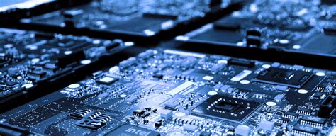
Printed Circuit Boards (PCBs) are the backbone of modern electronics, bridging the gap between electronic components and ensuring seamless operation. Understanding PCB design and assembly is crucial for engineers and manufacturers seeking to create reliable, efficient products. In this realm, pcba—the term commonly used for the printed circuit board assembly—plays a pivotal role, encompassing both the design intricacies and the intricate processes involved in assembling these essential components. The design phase requires a keen attention to detail; it involves selecting optimal layouts that promote signal integrity and facilitate thermal management while effectively utilizing board space. Subsequently, the assembly phase involves placing components on the PCB through various methods like surface mount technology (SMT) or through-hole techniques, which are essential for producing high-quality electronics. A thorough understanding of these processes not only enhances product performance but also contributes to the overall efficiency in electronics production. By mastering these foundational aspects of PCB design and pcb assembly, professionals can ensure that they meet industry standards while fostering innovation in electronic devices. Through this guide, we will delve deeper into both realms, focusing on fundamental principles that govern successful PCB production workflows.
Key Components of Effective PCB Design
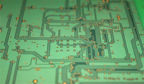
An efficient PCB design entails understanding and integrating several key components that directly influence both performance and manufacturability. At the heart of any successful pcb assembly process is a well-structured layout, which begins with a clear understanding of the electrical requirements and intended functionality. Essential components include effective use of ground planes, which significantly reduce electromagnetic interference (EMI) and improve signal integrity. Additionally, designers should prioritize component placement to minimize trace lengths, thus enhancing the overall performance of the board.
The choice of materials is also crucial; using high-quality substrate materials can lead to better thermal management and durability in various environments. Integrating design for manufacturability (DFM) principles can streamline the transition from design to production, enabling smoother pcba processes. Moreover, consideration for the size and footprint of components can facilitate more compact designs without sacrificing connectivity or performance. Designers need to be adept at using simulation software that predicts potential issues early in the design stage, mitigating future complications during the assembly phase. Emphasizing these components not only contributes to high-quality results but also paves the way for more efficient workflows in electronics production, ensuring that each assembly meets rigorous standards and market demands effectively.
Best Practices for PCB Layout Optimization
When it comes to PCB layout optimization, several best practices can enhance both the performance and manufacturability of your designs. First and foremost, it’s essential to ensure a proper component placement that minimizes trace lengths, thereby reducing parasitic capacitance and inductance. This careful arrangement not only contributes to a more efficient signal path but also facilitates easier pcb assembly during manufacturing. Additionally, maintaining an appropriate balance between ground and power planes can significantly improve signal integrity, especially in high-frequency applications.
Another crucial aspect is the use of via strategies—choosing the right type and number of vias based on your design requirements can help prevent unwanted impedance changes within your circuit. Furthermore, utilizing adequate spacing between traces reduces the risk of electrical interference and improves overall reliability. Implementing design rules specific to your PCB manufacturer will also streamline production processes, ensuring that your PCBA meets quality standards right from the start.
"A well-optimized layout not only enhances efficiency but also plays a pivotal role in achieving high-quality results in your electronics production."
Incorporating these practices into your PCB layout will not only boost performance but also pave the way for streamlined workflows during the pcb assembly process. As you refine your designs with these considerations in mind, you’ll find that maintaining clear documentation throughout the design phase can aid communication with manufacturing partners and reduce production delays. Ultimately, adopting such best practices establishes a strong foundation for successful project outcomes in today’s competitive electronics landscape.
The Assembly Process: Techniques and Tools
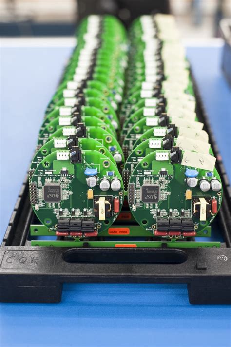
The pcb assembly process is a critical phase in electronics production, where individual components are placed and soldered onto a printed circuit board (PCB). Mastery of this stage requires a combination of techniques and tools that streamline operations and ensure precise results. One of the key techniques employed during pcba is surface-mount technology (SMT), which allows components to be mounted directly onto the surface of the PCB. This method is favored for its efficiency and ability to accommodate high-density layouts. Additionally, through-hole technology remains relevant for specific applications, where components are inserted into pre-drilled holes on the PCB.
In terms of tools, automated pick-and-place machines have revolutionized the pcb assembly process. These machines accurately position components on the board, drastically reducing assembly time while maintaining high precision. Complementing this, reflow ovens are essential for soldering the surface-mounted components through controlled heating, ensuring robust connections. Manual assembly, although less prevalent in high-volume environments, still plays a role in specialized applications where precision and care are paramount.
Proper training in both techniques and tool usage cannot be overstated; skilled operators who understand the nuances of pcba processes can significantly influence overall product quality. The integration of quality control measures throughout this stage—such as optical inspection systems—ensures that defects are caught early, leading to lower production costs and better reliability in the final product. Ultimately, adopting advanced technologies while adhering to best practices during the pcb assembly process is vital for producing efficient electronics that meet industry standards.
Quality Assurance in PCB Production
Quality assurance plays a pivotal role in the pcb assembly process, ensuring that each printed circuit board (PCB) meets rigorous standards before it is deployed in electronic devices. The importance of a robust quality assurance framework cannot be overstated; it encompasses the entire pcba lifecycle, from design validation to final inspections. By implementing systematic checks and balances during pcb design and assembly, manufacturers can detect potential flaws early on, minimizing costly rework and delays.
Key factors in maintaining quality assurance include regular testing of components and assemblies, adherence to industry standards, and employing advanced inspection technologies. Notably, acoustic microscopy and X-ray inspection are invaluable tools that help identify hidden defects within a pcba. Moreover, establishing clear documentation practices for each stage of production further reinforces quality by providing a traceable path for all materials used.
To elevate the quality assurance process, it is also essential to conduct thorough training for the workforce involved in pcb assembly. Employees should be well-versed in quality protocols and encouraged to adopt a mindset focused on continuous improvement. This proactive approach ultimately leads to the production of high-quality PCBs that not only meet but exceed customer expectations while enhancing overall operational efficiency. By prioritizing quality through comprehensive programs and technology integration, manufacturers can stay competitive in the dynamic landscape of electronics production.
Streamlining Workflows in Electronics Manufacturing
In the realm of PCB design and assembly, optimizing workflows is critical for achieving maximum efficiency and output quality. One effective approach involves the meticulous planning of the PCB layout, which facilitates smoother pcba processes and minimizes errors during assembly. Utilizing advanced software tools to simulate designs ensures that potential issues are addressed prior to the assembly phase. Moreover, standardizing components and techniques can significantly reduce time spent on production, allowing for quicker turnaround times while maintaining high standards of craftsmanship.
Additionally, automating repetitive tasks in the pcb assembly process can greatly enhance workflow efficiency. By incorporating robotics and automated systems, manufacturers can not only speed up production but also improve accuracy, which is essential for the integrity of pcba. Training personnel on these new technologies ensures that teams are well-equipped to handle the complexities of modern electronics manufacturing. Emphasizing open communication among team members during both design and assembly stages fosters a collaborative environment where innovative solutions can be developed swiftly.
Ultimately, focusing on these streamlined workflows within electronics manufacturing leads to a more cohesive operation that thrives on efficiency and productivity, paving the way for sustained growth in an ever-evolving industry.
Troubleshooting Common PCB Design Issues
When dealing with PCB design and assembly, it’s not uncommon to encounter various challenges that can impede the production process. Understanding these issues is crucial for efficient PCBA – the integration of both design and assembly. One common problem is related to design errors, which can range from incorrect component placement to inadequate trace widths that fail to support necessary current levels. Detecting these mistakes early in the process is essential; otherwise, they can lead to significant functional failures in electronic devices.
Another frequent issue lies in signal integrity. Issues arising from impedance mismatches or excessive crosstalk can lead to degraded performance in high-frequency applications. Employing techniques such as controlled impedance designs and using differential pairs can help mitigate these problems. Additionally, thermal management plays a vital role—overheating components can shorten lifespan or cause immediate failure if not adequately addressed in the PCBA phase.
Furthermore, alignments during assembly can also lead to failure if components are misplaced or solder joints are insufficiently robust. Maximizing automation and precision during assembly processes helps ensure that each component adheres correctly, resulting in high-quality outputs. By diligently troubleshooting these common PCB design issues, engineers can cultivate a more streamlined workflow and improve the overall efficiency of electronics production, ultimately leading to successful end products that meet market demands.
Future Trends in PCB Technology and Innovation
As technology continues to evolve, the field of PCB design and assembly is witnessing groundbreaking advancements that promise to redefine electronic manufacturing. One of the most significant trends is the emergence of flexible PCBs, which enable designers to create devices that are thinner and lighter while maintaining stellar performance. This shift towards flexibility also supports a vast array of applications, from wearable technology to automotive systems, showcasing the versatility of pcb assembly techniques. Another notable trend is the integration of advanced materials, such as high-frequency substrates and eco-friendly choices, which enhance signal integrity and promote sustainability in production processes. Additionally, automation in pcba processes is becoming increasingly prevalent; employing robotics and machine learning algorithms allows for greater accuracy and efficiency in assembly lines. Furthermore, innovations in design software are streamlining workflows by offering advanced simulation tools that help engineers foresee potential issues before actual production begins. Collectively, these trends not only foster efficiency in electronics production but also pave the way for a more innovative future where PCB technology can meet the rising demands of both consumers and industries alike.
Conclusion
In wrapping up our exploration of PCB design and assembly, it is crucial to emphasize the importance of implementing effective strategies that enhance production efficiency within the realm of electronics manufacturing. Navigating the complexities of PCBA—the fusion of PCB design and assembly—requires not only a solid understanding of fundamental concepts but also a commitment to ongoing improvement. As we have examined, leveraging advanced tools, thorough layout optimization, and robust quality assurance processes significantly contributes to producing high-quality electronic products. The future landscape of PCB technology is poised for remarkable innovations, driven by continuous advancements in design methodologies and assembly techniques. By staying abreast of these changes and integrating best practices, manufacturers can ensure that their PCBA processes remain competitive and responsive to market demands. Ultimately, mastering these elements not only streamlines workflows but also empowers creators to deliver exceptional results—further underscoring the significance of skillfully navigating PCB design and assembly challenges in today’s fast-paced electronics environment.
FAQs
What is PCB assembly?
PCB assembly, often abbreviated as PCBA, refers to the process of assembling electronic components onto a printed circuit board (PCB). This crucial step ensures that the electronic components function correctly and are securely attached to the board.
What are the key steps involved in PCB assembly?
The key steps in PCB assembly include solder paste application, component placement, soldering (either manually or using automated techniques), inspection, and testing. Each step is vital to achieving a high-quality final product.
How does the quality assurance process work in PCBA?
Quality assurance in PCBA involves several testing methods, such as visual inspection, automated optical inspection (AOI), and functional testing. These tests ensure that each board meets specific standards and functions as intended.
What materials are commonly used for PCB components?
Common materials for PCB components include resistors, capacitors, integrated circuits, and various connectors. The choice of materials can impact performance, durability, and cost.
Why is layout optimization important in PCB design?
Layout optimization is essential because it directly affects both functionality and manufacturability. An optimized layout can reduce signal loss, improve thermal management, and streamline the assembly process, leading to more efficient production.
For more detailed information on PCB assembly, please click here: Andwin PCB Assembly.