PCB Solder Mask Design Guide: Color Selection, Solder Mask Bridge Design and Covering Process Analysis
When placing an order for a PCB, you will see two options related to solder mask: solder mask color and solder mask coverage. As shown in the figure below.
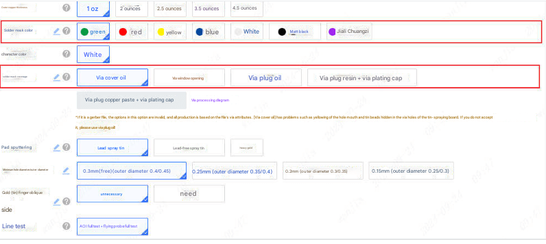
As the name suggests, these two options are closely related to solder mask.
As one of the key steps in PCB design and manufacturing, solder mask plays an important role.
It not only prevents the erosion of moisture and chemicals and avoids oxidation and corrosion of the circuit, but also protects the circuit from physical damage and maintains good insulation performance of the board surface. At the same time, solder mask can also prevent areas that should not be soldered from being connected by solder to avoid short circuits. In addition, beautifying the appearance and improving the visual effect of the PCB is also one of the functions of solder mask.
Today, let’s talk about solder mask color, solder mask bridge and solder mask coverage to help you avoid pitfalls when designing PCBs.
You can choose the solder mask color, but please consider carefully and don’t match it randomly.
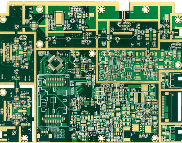
The most common PCB appearance is green, which looks like this:
Why is green the most common color, not red, white, blue or yellow?
This has to do with the history of PCB development. The solder mask materials commonly used in early PCB manufacturing contain brominated epoxy resin. The characteristic of this material is that it naturally appears green after curing. The appearance is as follows:

Brominated epoxy resin
On the other hand, green ink has good performance, has a good reaction in UV exposure, and can be cured more evenly. Moreover, in production and manufacturing, green ink not only has high visual contrast, which is convenient for checking circuits and solder joints and identifying defects, but also has stable performance. In addition, it can protect the operator’s eyesight and has little irritation to the eyes.
Therefore, over time, green has gradually become the most common PCB color in the industry with its excellent performance and reliability.
Nowadays, the appearance colors of PCBs are becoming more and more diverse. Taking Jiali Chuang as an example, seven solder mask ink colors are provided, namely green, red, yellow, blue, white, matte black and Jiali Chuang purple.
Although there are more optional colors, you should be careful when choosing. This is because different colors of ink react differently to light.
Imagine that a black T-shirt is hotter than a white T-shirt in the sun, because black absorbs more light and white reflects more. Similarly, different colors of solder mask ink absorb and reflect UV light (the light source used to cure the ink) differently.
If there are no special requirements, basically choose green.
Some people who have experienced it suggest that you should not mess around with the color of the ink. Choose green for daily use, which is commonly used, cheap, stable, and has a fast delivery time.
Of course, if it is an LED light board or an aluminum substrate, white ink is generally used to achieve the brightest reflected light; if it is to prevent the PCB from reflecting light, matte black will be used.
It is particularly worth noting that in the proofing stage, try not to make black, because the black oil board is not friendly to hardware engineers for debugging.
If you choose the same color (such as green) for different PCB manufacturers, you may find that although they are all green, they do not look exactly the same. This is because of color difference.
The occurrence of color difference is affected by many factors, including the ink used, production method, baking time, and screen printing speed.
Solder mask color difference factor
Therefore, if there are no special requirements for the PCB, it is recommended to choose the most commonly used green. If a certain ink color is required, be sure to indicate the ink manufacturer and ink model.
Say goodbye to welding short circuits and master the key points of solder mask bridge design
Solder mask ink not only determines the appearance color of the PCB, but is also closely related to the solder mask bridge.
Solder mask bridge
Solder mask bridge refers to the connecting part between adjacent pads on the PCB composed of solder mask ink. Its main function is to prevent abnormal flow of solder between pads, thereby avoiding short circuits.
In IC packages with small gaps, the importance of solder mask bridges is particularly prominent. It can effectively prevent solder adhesion during the SMT process and significantly improve the pass rate of soldering. This is crucial for the normal function realization and reliable operation of PCBs.
When designing a solder mask bridge, it is important to understand the process parameters of the PCB manufacturer. The following figure shows the minimum process parameters of the solder mask bridge of Jiali Chuang.
In the process of designing a solder mask bridge, the following points need to be noted:
● In IC package design, if the solder mask opening adopts an opening window design, the solder mask bridge cannot be realized.
● If the pad spacing is too small, forcibly requiring the manufacture of a solder mask bridge may lead to the risk of falling off.
●Avoid designing solder mask bridges at solder mask openings of contact button packages or PCBs with plug-in gold fingers
If more advanced production technology is used, some solder mask bridge problems can be avoided. For example, Jiali Chuang uses advanced LDI exposure technology in the production of high-layer PCBs, and directly images CAM data on the PCB through laser scanning. This method reduces the deviation caused by film expansion and contraction, improves alignment accuracy, and greatly improves the production capacity of solder mask bridges.
Four types of solder mask coverage, which one is suitable for you
The solder mask coverage process is one of the important links in PCB manufacturing, and different coverage methods are suitable for different application scenarios. Taking Jiali Chuang as an example, four solder mask coverage methods are provided, namely via cover oil, via window, via plug oil and plate hole process.
Via cover oil
If you are designing a double-sided board with low demand for via filling, via cover oil is an economical and efficient choice. This method has a low production cost and is relatively simple to operate, but some vias may not be fully covered with oil, resulting in yellowing of the hole mouth, and tin beads are easily hidden in the hole under the tin spraying process.
Via windowing
The advantage of via windowing is that it is conducive to the transmission of large current and heat dissipation of vias, and the production is relatively convenient, but the disadvantage is that the reliability is reduced, and there may be hidden dangers such as tin leakage and tin short circuit. This process is suitable for PCBs with relatively simple functions, large current transmission or plug-in components.
Via plugging oil
For high-frequency PCBs with high-density wiring or high requirements for via filling, via plugging oil is more suitable. Its advantages include reducing yellowing of the hole mouth, enhancing electrical insulation performance, reducing signal interference, and improving the overall appearance consistency and reliability of the PCB. However, this process is relatively complex and costly, and if the vias on the pads are not properly processed, the ink may penetrate to the other side, affecting the welding quality.
Pad-in-hole process
When the PCB space you design is limited and the wiring is difficult, especially for high-layer boards, it is suitable to choose the pad-in-hole process.
It can not only improve the efficiency of PCB design engineers and further improve the yield of PCBs, but also provide more wiring space. Especially when BGA wiring, this process can significantly improve electrical performance.
In the past, this process was widely considered a “luxury” due to its high cost, but as Jiali Chuang waives the via-in-pad process fee (resin plugging + electroplating capping) for 6-32 layer high multi-layer PCBs, more products can use this process.
In addition, there are some design rules to pay attention to when using the via-in-pad process. For example, a 0.3mm BGA is suitable for a 0.2mm hole, and a 0.45mm BGA pad is suitable for a 0.3mm hole. The maximum hole diameter should not exceed 0.5mm, and the minimum hole diameter is recommended to be no less than 0.2mm.
Finally, it should be pointed out that solder mask ink also has a great influence on the signal transmission of the outer layer of the PCB. When designing high-speed PCBs, the signal loss will increase after the surface of the microstrip line is covered with solder mask ink. The thicker the solder mask ink, the greater the signal loss.
Therefore, it is recommended to use solder mask ink with a smaller dielectric constant (ε) and dielectric loss factor (DF) for high-speed PCB design, and the thickness of the solder mask ink printing should be as small as possible to ensure better signal transmission effect.
Some articles on this site are reprinted or posted by netizens for the purpose of transmitting and sharing information. This does not mean that this website agrees with their views and is responsible for their authenticity; the copyright of the article belongs to the original author and the original source. If it involves the content, copyright and other issues of the work, we will correct or delete it as soon as possible according to the requirements of the copyright owner.
Netizen comments