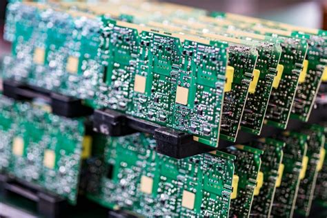
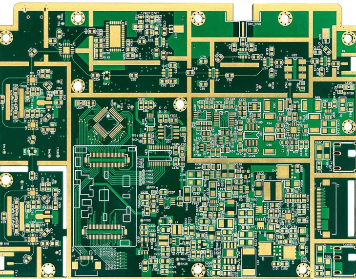
Effective countermeasures for PCB process film deformation
In the PCB copying process, the temperature and humidity control fails or the temperature of the exposure machine rises too high, sometimes causing the film to deform. If it is not improved, the quality and performance of the final PCB copy board will be affected, but direct abandonment will cause cost losses. Then mastering the correction process of film deformation will make the work better. The editor has summarized five simple and commonly used methods for everyone to pick up and use when needed. The following is for reference only. The specific measures will depend on the basics. It depends.
1.Splicing method
For graphics with simple lines, large line widths and spacing, and irregular deformation, cut the deformed parts of the film, re-join them according to the hole positions of the drilling test board, and then copy them. Of course, this is for simple deformed lines. , graphics with large line width and spacing and irregular deformation; not suitable for films with high wire density and line width and spacing less than 0.2mm. When splicing, be careful not to damage the wires as much as possible and not damage the pads. When revising the version after splicing and copying, pay attention to the correctness of the connection relationship. This method is suitable for films that are not too dense in circuits and have inconsistent deformation of the films on each layer. The effect is particularly obvious for the correction of solder mask films and power supply ground films of multi-layer boards.
2.PCB copy board changing hole position method
After mastering the operating technology of the digital programmer, first compare the negative film and the drilled test board, measure and write down the length and width of the drilled test board, and then use the digital programmer to measure the length and width of the drilled test board. According to the amount of deformation, adjust the hole position and adjust the drilled test plate to cater to the deformed negative film. The advantage of this method is that it eliminates the troublesome work of editing the negatives and ensures the integrity and accuracy of the graphics. The disadvantage is that the correction effect on negatives with very serious local deformation and uneven deformation is not good. To use this method, you must first master the operation of the digital programmer. After using the programmer to lengthen or shorten the hole positions, the hole positions that are out of tolerance should be reset to ensure accuracy. This method is suitable for correction of films with dense circuits or consistent deformation of films on each layer.
3.Pad overlap method
Enlarge the hole on the test board into a pad to overlap the deformed circuit piece to ensure the minimum ring width technical requirements. Because after overlapping copying, the pad becomes elliptical, and after overlapping copying, there is halo and deformation at the edge of the line and pad. If the user has very strict requirements on the appearance of the PCB board, please use it with caution. This method is suitable for films with line width and spacing greater than 0.30mm and graphics lines that are not too dense.
4.Photography
Just use the camera to enlarge or reduce the deformed graphics. Usually the negative film has a lot of losses and requires multiple debugging to obtain a satisfactory circuit pattern. When taking photos, focus must be accurate to prevent line deformation. This method is only applicable to silver salt films. It can be used when it is inconvenient to re-drill the test plate and the deformation ratio of the length and width of the film is consistent.
5.Hanging method
In view of the physical phenomenon that the film changes with the change of ambient temperature and humidity, take the film out of the sealed bag before copying and hang it in the working environment for 4-8 hours, so that the film will be deformed before copying. After copying, the chance of deformation is very small. For negatives that have been deformed, other methods need to be taken. Because the film will change with the changes in ambient temperature and humidity, when hanging the film, make sure that the humidity and temperature of the hanging place and the working place are consistent, and it needs to be in a ventilated and dark environment to prevent the film from being contaminated. This method is suitable for films that have not yet been deformed, and can also prevent the film from being deformed after copying.
Of course, the above are all remedial methods after the film is deformed. Engineers should still consciously prevent film deformation. In the PCB copying process, the temperature is usually strictly controlled at 22±2℃ and the humidity is 55%±5%RH. Use a cold light source or an exposure machine with a cooling device, and constantly replace backup films