How much do you know about impedance matching in high-frequency and high-speed PCB design?
With the rapid development of high-frequency and high-speed electronic products, signal transmission is more prone to signal integrity problems such as reflection and crosstalk. The higher the frequency and the faster the transmission rate, the more serious the signal loss. How to reduce the loss of the signal during transmission and ensure signal integrity is a huge challenge in the development of high-frequency and high-speed PCB.
In high-speed PCB design, impedance matching is particularly important. In order to reduce the reflection phenomenon during high-speed signal transmission, impedance matching must be maintained at the signal source, receiving end and transmission line.
Generally speaking, the impedance of a single-ended signal line depends on its line width and relative position to the reference plane. The line width/line spacing between differential pairs required by characteristic impedance depends on the selected PCB stacking structure.
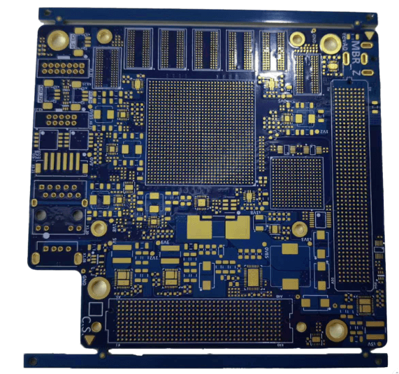
Since the minimum line width and minimum line spacing depend on the PCB type and cost requirements, the selected PCB stacking structure must be able to meet all impedance requirements on the board, including inner and outer layers, single-ended and differential lines, etc. For PCB factories, boards with impedance lines are commonly called impedance boards.
Factors affecting impedance
In the design of high-speed PCBs, experienced engineers have a certain understanding of PCB materials and process technology, and know the relevant parameters that affect impedance. They will use impedance software such as Si9000 or Huaqiu DFM in advance to select the corresponding impedance model for impedance meter, so as to obtain the impedance matching of PCB. However, to truly achieve the expected characteristic impedance or actually control it within the expected characteristic impedance value range (usually within ±10%), it can only be achieved through the management and control of the PCB production process.
From the perspective of PCB manufacturing, the key factors affecting impedance are mainly:
Key factors affecting
Dielectric thickness (h): Increasing dielectric thickness can increase impedance, and reducing dielectric thickness can reduce impedance; for multi-layer boards, dielectric thickness depends on the thickness of PP sheets and core boards.
Line width (w): Impedance is inversely proportional to line width. The larger the line width, the smaller the impedance. Generally speaking, the line width tolerance of the impedance line should be controlled to 5%-10% during the production process.
Copper thickness (t): Reducing the line thickness can increase the impedance, and increasing the line thickness can reduce the impedance. The finished copper thickness of the line is related to the selected base copper foil and the electroplating process.
Dielectric constant (Er): Different boards have different dielectric constants. Increasing the dielectric constant can reduce the impedance, and reducing the dielectric constant can increase the impedance.
Solder mask thickness (c): Printing solder mask will reduce the outer layer impedance. Under normal circumstances, printing one solder mask can reduce the single-ended by 2 ohms and the differential by 8 ohms. The reduction value after printing two times is twice that of one time. When printing more than three times, the impedance value will no longer change.
From the above factors, it can be seen that, limited by the appearance of electronic products, circuit conduction, signal stability and heat dissipation performance, generally speaking, the PCB designed by engineers has relatively fixed number of layers, board thickness, copper thickness and size. Therefore, it can be seen that the impedance of the produced PCB must match the designed impedance and control the tolerance within ±10. The adjustable parameters are mainly line width, core copper foil thickness, PP sheet dielectric constant, and stacking structure.
Basic principles of stacking design
For PCB board factories, they generally cooperate with 2-3 material brand manufacturers to select several types of PP and core copper foil as raw materials for PCB, and make stacking designs according to the factory’s process capabilities and production processes, and match the corresponding impedance. Generally speaking, different stacking structures can be used for multiple impedance matching. The final choice of impedance matching depends on whether the PCB wiring is reasonable, the interference between signals, etc., and is also limited by the final PCB cost. Line width is too small, buried blind holes, etc. will affect the final cost.
There are some basic principles for stacking design here:
Stacking is symmetrical
Impedance continuity
Ground layer under the component (2nd layer or 2nd to last layer)
Power supply is tightly coupled with ground
Signal layer is close to reference layer
Adjacent signal layers are spaced farther apart
When the signal layer is sandwiched between the power layer and the ground layer, the signal layer is close to the ground layer
Differential spacing ≤ 2 times the line width
Line width adjustment within the range of 4-6mil
Prepreg (PP) ≤ 3 sheets between board layers
At least one sheet of 7628, 3313 or 2116 is required for the secondary outer layer
Prepreg use order 7628→2116→3313→1080→106
Here we have to mention a PCB manufacturability analysis and PCBA assembly analysis artifact – Huaqiu DFM, which is a PCB manufacturability analysis software independently developed by Huaqiu Electronics. As a free domestic software, it can automatically generate stacking diagrams, or manually fill in the number of layers, board thickness, copper thickness, and use the dielectric thickness of the stacking diagram to match impedance. It is convenient for engineers to obtain more system margins from more optimized PCB designs to resist processing errors, and it is also possible to predict production costs in advance.
Huaqiu has something to say about whether the impedance board is highly reliable
After the PCB design is completed, it is necessary to verify whether the solution is feasible and whether the product is reliable.
In the end, it is not known until it is produced. How does Huaqiu do it for PCBs with impedance? There are usually two situations
The first is that the customer provides PCB files, which have clearly defined impedance requirements and stacking structures, and allow for small adjustments.
In this case, engineering design generally checks whether the process capability can be met and whether the stacking design can be realized.
If it is fully matched, the subsequent steps can be carried out according to the file; if a small range of adjustment is required, engineering design will adjust the impedance design according to the type of its own board, PP type, line width within the process capability range, and production process to meet customer needs.
The second is that the customer provides PCB files with requirements for impedance, but does not specify the stacking structure.
In this case, engineering design generally gives priority to the recommended stacking structure to match the corresponding impedance.
Why is the stacking structure preferred? There are two reasons:
First, the laminated structure recommended by Huaqiu has been verified by more than 10 years of mature production. The board performance, production process, and process control are all proven, thus ensuring the high reliability of the product. It is understood that 90% of customers will choose the laminated structure recommended by Huaqiu, and the product has also been recognized by the majority of customers.
Second, the laminated structure recommended by Huaqiu can maximize the use of the board, provide board utilization, thereby reducing production costs and ensuring the consistency of product quality. Friends who have learned about Huaqiu know that Huaqiu PCB is mainly for proofing and small and medium batches. For this kind of flexible production PCB board factory, it is generally used to combine multiple PCBs together by paneling. Obviously, the board utilization rate has increased, which means lower costs for customers; on the other hand, the combined PCB board, if a relatively consistent laminated structure is used, can improve product quality in the lamination process.
The following figure is one of the laminated structures recommended by Huaqiu. For more laminated designs, please refer to Huaqiu DFM impedance calculation, or refer to the laminate recommended by Huaqiu PCB official website.
After the PCB determines the stacking structure and impedance matching, the final step is to produce the PCB; in the PCB production and processing stage, Huaqiu has a comprehensive quality management system to ensure the high reliability of the product.
Raw material side: high-quality raw materials, Jiantao/Shengyi A-grade boards
Production side: mature manufacturing process, high-precision equipment and standardized equipment management
Quality control side: comprehensive quality management system, real-time data collection of key processes, detection and analysis
Management side: professional training, standardized operation promotion, human-machine interconnection, abnormal warning
System side: complete system certificates, ISO9001, ISO14001, RoHS, IATF16949, UL, CQC, REACH