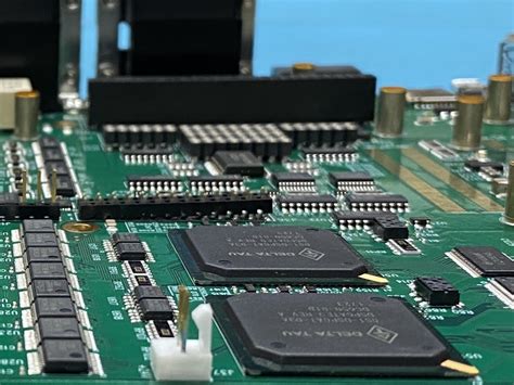
High-speed PCB copy board and PCB design strategy
Currently, high-speed PCB design is widely used in the fields of communication, computer, graphics and image processing. The high-speed PCB design strategies used by engineers in these fields are also different.
In the field of telecommunications, the design is very complex
The transmission speed in data, voice and image transmission applications is far higher than 500Mbps. In the field of communications, people pursue faster launch of higher-performance products, and cost is not the first priority. They will use more board layers, sufficient power layers and ground layers, and use discrete components to match any signal lines that may have high-speed problems. They have SI (signal integrity) and EMC (electromagnetic compatibility) experts to perform simulation and analysis before wiring, and every design engineer follows the strict design regulations within the company. Therefore, design engineers in the field of communications usually adopt this over-designed high-speed PCB design strategy.

Motherboard design in the field of home computers is another extreme. Cost and effectiveness are above all else.
Designers always use the fastest, best, and highest-performance CPU chips, memory technology, and graphics processing modules to form increasingly complex computers. Home computer motherboards are usually 4-layer boards, and some high-speed PCB design technologies are difficult to apply to this field. Therefore, engineers in the field of home computers usually use an over-research method to design high-speed PCB boards. They need to fully study the specific design conditions to solve the real high-speed circuit problems.
The usual high-speed PCB design situation may be different.
Manufacturers of key components (CPU, DSP, FPGA, industry-specific chips, etc.) in high-speed PCBs will provide design information about the chips, which are usually given in the form of reference designs and design guidelines. However, there are two problems here: first, there is a process for device manufacturers to understand and apply signal integrity, and system design engineers always want to use the latest high-performance chips at the first time, so the design guidelines given by device manufacturers may not be mature. Therefore, some device manufacturers will give multiple versions of design guidelines at different times. Secondly, the design constraints given by device manufacturers are usually very harsh, and it may be very difficult for design engineers to meet all design rules. In the absence of simulation analysis tools and the lack of understanding of the background of these constraint rules, meeting all constraints is the only means of high-speed PCB design. Such a design strategy is usually called over-constraint.
An article mentioned that a backplane design uses surface mounted resistors to achieve terminal matching.
More than 200 such matching resistors are used on the circuit board. Imagine if you want to design 10 prototypes to ensure the best terminal matching effect by changing these 200 resistors, it will be a huge workload. And it is really surprising that no change in the resistor value in this design benefits from the analysis results of SI software.
Therefore, it is necessary to add high-speed PCB design simulation and analysis to the original design process, making it an indispensable part of complete product design and development.


