What kind of layout can achieve heat dissipation?
There are three main sources of heat in PCB:
(1) heat generated by electronic components;
(2) heat generated by the PCB itself;
(3) heat transmitted from other parts.
Among these three heat sources, the heat generated by components is the largest and is the main heat source, followed by the heat generated by the PCB board. The heat transmitted from the outside depends on the overall thermal design of the system and is not considered for the time being. The purpose of thermal design is to take appropriate measures and methods to reduce the temperature of components and the temperature of the PCB board so that the system can work normally at an appropriate temperature. The following aspects can be considered:
1.Heat dissipation through the PCB board itself.
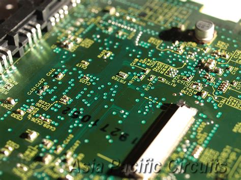
The widely used PCB board materials at present are copper-clad/epoxy glass cloth substrates or phenolic resin glass cloth substrates, and a small amount of paper-based copper-clad boards are also used.
Although these substrates have excellent electrical properties and processing properties, they have poor heat dissipation. As a heat dissipation path for high-heat components, it is almost impossible to expect the PCB resin to conduct heat, but to dissipate heat from the surface of the component to the surrounding air.
However, as electronic products have entered the era of miniaturization of components, high-density installation, and high-heat assembly, it is not enough to rely solely on the surface of components with very small surface areas to dissipate heat. At the same time, due to the large-scale use of surface-mounted components such as QFP and BGA, the heat generated by the components is transferred to the PCB board in large quantities. Therefore, the best way to solve the heat dissipation problem is to improve the heat dissipation capacity of the PCB itself that is in direct contact with the heat-generating components, and conduct or dissipate it through the PCB board.
2.Add heat sinks and heat conduction plates to high-heat-generating components.
When a few components in the PCB generate a large amount of heat (less than 3), a heat sink or heat pipe can be added to the heat-generating component. When the temperature cannot be lowered, a heat sink with a fan can be used to enhance the heat dissipation effect. When there are a large number of heat-generating components (more than 3), a large heat dissipation cover (plate) can be used. It is a special heat sink customized according to the position and height of the heat-generating components on the PCB board, or different component height positions are cut out on a large flat heat sink. The heat dissipation cover is buckled on the component surface as a whole, and it contacts each component to dissipate heat. However, due to the poor height consistency of components during soldering, the heat dissipation effect is not good. Usually, a soft thermal phase change thermal pad is added to the component surface to improve the heat dissipation effect.
3.Use reasonable routing design to achieve heat dissipation.
Since the resin in the board has poor thermal conductivity, and the copper foil lines and holes are good conductors of heat, increasing the copper foil surplus rate and increasing the thermal conductive holes are the main means of heat dissipation.
4.When high heat dissipation devices are connected to the substrate,
the thermal resistance between them should be reduced as much as possible. In order to better meet the thermal characteristics requirements, on the circuit board. Air always tends to flow to places with low resistance when flowing, so when configuring devices on the printed circuit board, avoid leaving a large airspace in a certain area. The configuration of multiple printed circuit boards in the whole machine should also pay attention to the same problem.
5.Devices that are sensitive to temperature are best placed in the lowest temperature area (such as the bottom of the device).
Never place it directly above the heating device. Multiple devices are best arranged in a staggered manner on the horizontal plane.
6.Avoid the concentration of hot spots on the PCB, distribute the power evenly on the PCB board as much as possible
and keep the temperature performance of the PCB surface uniform and consistent. It is often difficult to achieve strict uniform distribution during the design process, but it is necessary to avoid areas with too high power density to avoid overheating and affect the normal operation of the entire circuit.