Maximizing Efficiency with Breakout PCBs in Your Circuit Designs
Key Takeaways
Understanding the significance of breakout PCBs in your design process can elevate the efficiency of your circuits significantly. Breakout PCBs facilitate optimal power distribution, which is crucial for ensuring that each component receives the appropriate voltage and current. By leveraging pcb manufacturing advancements, you can implement these specialized boards in your projects with greater ease and effectiveness. When exploring potential pcb manufacturing companies, it’s essential to consider their expertise in producing high-quality breakout designs tailored to your specific needs. This not only impacts the pcb manufacturing cost, but it also plays a vital role in the overall performance and reliability of your electronic designs. Well-integrated breakout PCBs help mitigate common electrical issues, making them a preferred choice in many designs today. As you navigate through different aspects of your pcb manufacturing business, keep in mind that adopting best practices for designing efficient breakout PCBs will contribute positively to both project timelines and outcomes. Thus, making informed decisions about your PCB choices will ultimately lead to more successful implementations in real-world applications.

Introduction to Breakout PCBs and Their Importance in Circuit Design
When designing circuits, understanding the role of breakout PCBs is crucial for enhancing performance, particularly in power distribution. A breakout PCB allows multiple connections to be made from a single point, creating a streamlined pathway for electrical signals. This is essential as it reduces the complexity of your circuit by minimizing the number of wire connections and potential points of failure. In your circuit designs, employing breakout PCBs can help optimize space and improve signal integrity, which are key factors in achieving reliability.
Moreover, considering the cost-efficiency of pcb manufacturing, it is vital for you to choose components that enable better integration and lower production costs. With many pcb manufacturing companies offering specialized services tailored for breakout designs, you can capitalize on their expertise to reduce your overall pcb manufacturing cost. Initiating a collaboration with a proficient pcb manufacturing business will allow you access to advanced technologies that enhance your design capabilities.
"Utilizing breakout PCBs is about embracing efficiency—both in design complexity and overall production costs."
By incorporating these techniques into your circuit layout, you not only streamline the power distribution but also improve the overall functionality of your electronic projects. This understanding lays the groundwork for deeper exploration into the benefits and best practices associated with using breakout PCBs effectively. As you continue designing, keep these principles in mind to elevate both performance and reliability in your work.
Key Benefits of Using Breakout PCBs for Power Distribution
Breakout PCBs offer significant advantages that can greatly enhance your circuit designs, particularly in the area of power distribution. One of the primary benefits is their ability to simplify the connection between various components, which can lead to improved overall performance. By using a breakout PCB, you can effectively manage power distribution across different areas of your circuit, thereby minimizing voltage drops and ensuring your components receive the power they need without unnecessary losses. Additionally, this streamlined approach allows for better thermal management, as heat can be dissipated more efficiently when components are properly spaced and organized.
Another advantage is flexibility during pcb manufacturing; many pcb manufacturing companies offer custom breakout PCB designs that cater to specific project requirements. This flexibility can significantly reduce pcb manufacturing costs, as you are less likely to encounter issues that require rework or redesign. Furthermore, employing breakout PCBs can enhance the reliability of your projects by providing a robust platform for connections that reduces susceptibility to failure points often found in more conventional layouts.
Integrating breakout PCBs into your designs not only simplifies assembly but also promotes an organized structure, which is vital for troubleshooting and maintenance. As you grow your pcb manufacturing business, focusing on these advanced techniques can give you a competitive edge in delivering high-quality products that meet stringent performance requirements while also being cost-effective. Embracing the benefits of breakout PCBs means investing in a technology that promises to maximize efficiency throughout your designs, ensuring reliable operations across various applications.
Effective Integration Techniques for Breakout PCBs
To achieve optimal performance when integrating breakout PCBs into your circuit design, you must consider several techniques that enhance both functionality and efficiency. One key approach is to ensure well-planned power distribution. By strategically positioning your breakout board in relation to the main circuitry, you can minimize the length of traces, thereby reducing resistance and improving signal integrity. This is especially vital when coordinating with various PCB manufacturing companies, as a thoughtful layout can significantly lower the overall PCB manufacturing cost and ensure that the final product meets your design specifications.
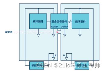
Another critical aspect is managing ground planes effectively. By linking the ground connections from various components to a common ground on the breakout PCB, you create a stable reference point that mitigates noise and enhances signal performance. In this context, understanding the nuances of pcb manufacturing processes can empower you to make informed decisions regarding material selection and board thickness, which directly influence reliability.
Remember that each decision in your design affects not just functionality but also budget considerations. Engaging with experienced professionals in the pcb manufacturing business can help streamline this process. They often provide invaluable insights into optimizing layouts while keeping production costs at bay. For instance, using advanced soldering methods can facilitate better connections and decrease defects during assembly.
For more information on integrating breakout PCBs into your designs effectively, you may want to explore options from reputable sources such as Andwin PCB Assembly. Ultimately, a thoughtful integration approach will elevate your circuit’s efficiency while promising long-term reliability.
Best Practices for Designing Efficient Breakout PCBs
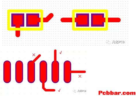
When designing efficient breakout PCBs, there are several best practices to keep in mind that can significantly enhance the performance and reliability of your circuit. Firstly, proper layout is crucial; ensuring that traces are kept as short and direct as possible minimizes resistance and inductance, which is vital for power distribution. Additionally, consider the use of via placements strategically. Placing vias close to components can reduce the amount of trace needed and provide a more stable connection.
Furthermore, utilizing a multi-layer PCB design can help to separate power and ground planes from signal traces, reducing noise and improving signal integrity. It’s also essential to take into account the pcb manufacturing cost when selecting materials—high-quality materials may have a slightly higher price, but they drastically improve durability and performance in the long run.
Collaborating with reliable pcb manufacturing companies can yield optimal results. These companies will provide insights into their capabilities regarding your design criteria, ensuring that your breakout PCB meets specific requirements without overshooting the budget on unnecessary enhancements. Additionally, during the prototyping phase, conducting rigorous testing will help identify potential issues early on in your design process before full-scale production begins.
Incorporating these strategies not only maximizes efficiency but also ensures that you are positioned well within the competitive pcb manufacturing business, providing you with a strategic advantage in your future projects. Overall, by aligning your design practices with these best practices for breakout PCBs, you enhance power distribution capabilities while maintaining cost-effectiveness throughout the design and manufacturing stages.
Real-World Applications of Breakout PCBs in Electronic Projects
Utilizing breakout PCBs in your electronic projects can lead to significant improvements in both organization and functionality. These boards are particularly beneficial when it comes to power distribution across complex circuit designs. By simplifying connections, they allow for a more streamlined layout, which can reduce the overall pcb manufacturing cost. This cost efficiency is crucial, especially for hobbyists and professionals alike, who often turn to various pcb manufacturing companies for their project needs.
In practical applications, breakout PCBs are widely used in both prototyping and production environments. For example, in robotics projects, using a breakout PCB can facilitate easier integration of sensors and actuators. The modular nature of these boards allows for quicker adjustments and replacements without the need for extensive rewiring. As your projects become more sophisticated, you’ll find these tools invaluable for maintaining system integrity and enhancing performance.
Moreover, within the pcb manufacturing business, there is a growing trend that highlights the importance of breakout boards in supporting additional components such as microcontrollers or specialized signal processing chips. This versatility not only maximizes the performance of your circuits but also aligns with modern design philosophies that prioritize efficiency and reliability.
Incorporating breakout PCBs into your electronic designs will thus empower you to achieve enhanced capabilities while minimizing unnecessary complexity. This ensures that whether you’re building a simple device or an intricate system, you’re equipped with the right tools to push your projects towards success.
Troubleshooting Common Issues with Breakout PCBs
When working with breakout PCBs, you may encounter several issues that can affect your circuit’s performance and reliability. One common challenge is poor signal integrity, which can arise from improper routing or inadequate grounding. To mitigate this, ensure that the traces are appropriately sized and spaced, and that grounding pads are connected to a solid ground plane. Another issue is the inconsistent voltage distribution across connections; this can be alleviated by using a well-planned layout that minimizes voltage drop, particularly when integrating larger power components. Additionally, be mindful of the pcb manufacturing cost associated with complex designs – intricate layouts may lead to higher expenses when choosing from various pcb manufacturing companies. Understanding the specifications and standards of your chosen pcb manufacturing business can significantly enhance your design’s success. If you notice overheating components, reevaluating the power distribution and layout makes all the difference; consider using thermal vias or creating larger pads for better heat dissipation. By addressing these common issues meticulously, you can maximize the efficiency of your projects and ensure a smoother workflow in your designs involving breakout PCBs.
Future Trends in Breakout PCB Development and Usage
As the landscape of electronics evolves, the development and usage of breakout PCBs are expected to follow suit. One of the notable trends is the increased focus on miniaturization and integration. As devices become smaller, your circuit designs will require breakout PCBs that not only conserve space but also enhance performance. Additionally, there is a growing emphasis on sustainability in PCB manufacturing processes. You might find that many PCB manufacturing companies are adopting eco-friendly materials and practices, which not only reduces waste but also decreases production costs. This shift can influence your decisions when choosing a manufacturing partner for your circuit designs.
Moreover, advancements in technology are paving the way for smarter breakout PCBs. With the integration of IoT devices, these boards will support better communication between components, making them integral to data-driven applications. Your projects may benefit from such innovations as they often lead to enhanced performance and efficiency.
Furthermore, as demand for custom solutions increases, you will notice that many PCB manufacturing businesses are offering more tailored options. This flexibility may allow you to create designs suited specifically to your unique project requirements while optimizing overall PCB manufacturing costs.
In summary, keeping an eye on these trends can help you leverage advancements in breakout PCB development, ensuring that your circuit designs remain competitive and effective in an ever-evolving market.
Conclusion
In conclusion, utilizing breakout PCBs can significantly enhance the efficiency and performance of your circuit designs. By integrating these specialized boards, you streamline power distribution, allowing for more organized and effective setups that can handle higher demands. It’s crucial to leverage insights from pcb manufacturing to ensure you choose quality materials, which contributes to the durability of your designs. Engaging with reputable pcb manufacturing companies will also help you keep your pcb manufacturing cost in check while guaranteeing top-notch standards. As you embark on your pcb manufacturing business, remember the importance of optimizing each design choice for both functionality and sustainability. Adopting best practices in breakout PCB design can pave the way for innovative solutions in your electronic projects, ensuring that you not only meet project requirements but also surpass expectations in terms of reliability and performance.
FAQs
What are breakout PCBs and how do they differ from standard PCBs?
Breakout PCBs are specialized circuit boards designed to facilitate connections between integrated circuits and other components. Unlike standard PCBs, which serve general purposes, breakout PCBs are optimized for efficient routing of signals and power distribution, making them essential for complex designs.
How can I benefit from using breakout PCBs in my designs?
Using breakout PCBs can enhance the performance and reliability of your circuits by simplifying connections, reducing noise interference, and improving overall layout efficiency. This leads to lower PCB manufacturing costs as fewer adjustments may be necessary post-production.
Are there specific integration techniques for breakthrough PCB designs?
Yes, effective integration techniques involve ensuring that PCB manufacturing companies follow precise specifications that allow for optimal component placement and minimal trace lengths. Techniques such as using smaller vias or aligning component footprints can greatly enhance efficiency.
What should I consider when designing a breakout PCB?
When designing a breakout PCB, focus on the layout to minimize inductance and resistance, which directly affects power distribution. Additionally, understanding pcb manufacturing business processes can help you select materials and follow design guidelines that keep costs down while maximizing performance.
Can I apply breakout PCB technology in any electronic project?
Breakout PCBs are versatile; they find application in a wide range of electronic projects—from prototyping new concepts to final product development. However, ensure that your design requirements justify the implementation of a breakout configuration rather than using simpler alternatives.