Advancements in PCB Fabrication and Assembly Processes
Key Takeaways
Advancements in PCB fabrication and assembly processes have revolutionized the electronics manufacturing landscape, driving improvements in productivity and quality. The integration of new materials and innovative techniques has allowed for significant enhancements in the robustness and performance of printed circuit boards (PCBs). One crucial aspect is the refinement of pcba workflows, which utilize advanced automated systems to streamline the fabrication process. As companies adopt these technologies, the emphasis on precision has increased, allowing for the production of more complex designs with tighter tolerances.
Furthermore, sustainability is becoming a critical consideration in PCB production. Manufacturers are exploring eco-friendly materials and processes that minimize waste without compromising performance. This trend not only meets regulatory demands but also aligns with consumer preferences for greener products.
Sharing insights from industry leaders can provide valuable guidance on best practices:
"Embracing technology while focusing on sustainability will define successful PCB manufacturing in the coming years."
Overall, staying abreast of these technological advancements is essential for engineers and manufacturers aiming to remain competitive in a rapidly evolving market.
Introduction to PCB Fabrication and Assembly: A New Era of Innovation
The landscape of PCB fabrication and assembly is undergoing a remarkable transformation fueled by innovations that enhance production capabilities and accuracy. As technology advances, the demand for high-performance printed circuit boards (PCBs) continues to rise, pushing manufacturers to adopt more sophisticated methodologies. The integration of new materials, such as high-frequency laminates and flexible substrates, is pivotal in creating PCBs that meet the rigorous requirements of modern electronics. Additionally, the incorporation of advanced techniques like laser direct imaging (LDI) and automated optical inspection (AOI) contributes significantly to improving both the quality and efficiency of the pcba process. Automation plays a crucial role as well; with robotic assembly systems becoming increasingly prevalent, manufacturers can achieve higher throughput while reducing human error. Consequently, these advancements are not only streamlining production but also redefining how designers approach PCB layouts, leading to innovative solutions that cater to dynamic market needs. As we venture further into this new era, understanding these developments in pcb assembly, combined with a focus on sustainability through environmentally friendly processes, will be essential for maintaining competitiveness in today’s fast-paced electronics industry.
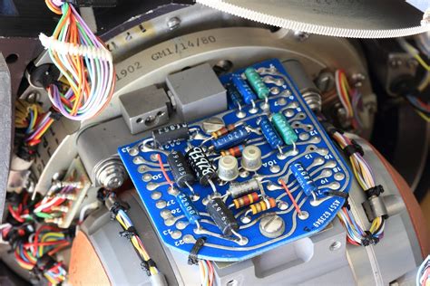
Key Materials Transforming PCB Production
The landscape of PCB fabrication and assembly is continuously evolving, driven by the introduction of advanced materials that significantly enhance the performance and reliability of printed circuit boards. One of the primary materials revolutionizing this domain is high-frequency laminate, which improves signal integrity in applications requiring swift data transmission. Additionally, the use of flexible substrates has enabled the production of lightweight and adaptable designs, suitable for intricate electronic devices or wearables.
Recently, innovations in solder materials, specifically lead-free solders, are gaining traction. These materials not only comply with environmental regulations but also provide superior mechanical properties crucial for high-reliability applications. Furthermore, advancements in conductive inks are promoting printable electronics, which allow for streamlined processes in PCB assembly, especially in lightweight applications.
The following table illustrates a comparison between traditional materials and emerging alternatives used in PCB production:
| Material Type | Traditional Material | Emerging Material |
|---|---|---|
| Substrate | FR-4 | High-frequency laminate |
| Solder | Tin-lead | Lead-free solder |
| Conductive Ink | Standard metal traces | Silver nano-particle inks |
| Flexibility | Rigid substrates | Flexible substrates |
Through the utilization of these innovative materials, manufacturers can attain higher levels of efficiency while ensuring greater precision during both pcb assembly and production processes. The integration of these modern materials leads to more durable, robust PCBs that meet the growing demands of various industries, ranging from consumer electronics to aerospace applications. As these transformations continue to unfold, they pave the way for a new frontier in PCB technology that is not only efficient but also environmentally conscious.
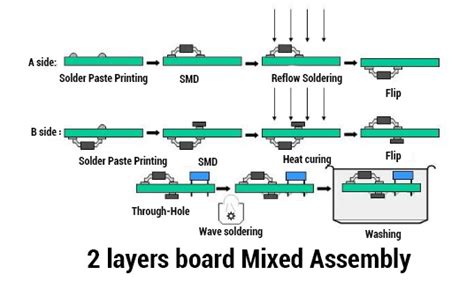
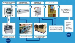
Advanced Techniques in PCB Fabrication: Enhancing Efficiency
The landscape of PCB fabrication is undergoing significant transformation, driven by the emergence of advanced techniques that not only streamline production but also elevate quality and precision. One notable technique gaining traction is the integration of laser technology, which enables meticulous etching and drilling that reduces waste and enhances accuracy in circuit design. Furthermore, the use of automated precision placement machines in PCB assembly ensures that components are placed with unparalleled accuracy, mitigating the risks associated with human errors during the assembly phase. These processes ensure that PCBA (Printed Circuit Board Assembly) achieves higher yields, facilitating quicker turnaround times while adhering to stringent quality standards. Additionally, high-frequency materials have become pivotal in meeting the demands for faster signal transmission and improved thermal management in complex electronic devices. By employing these innovative materials and techniques, manufacturers are poised to enhance operational efficiency significantly while catering to a growing market’s diverse needs. As technology progresses, it becomes increasingly clear that embracing these advancements is not merely beneficial but essential for staying competitive in the dynamic field of PCB production.

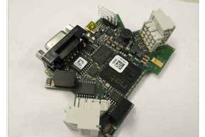
The Role of Automation in PCB Assembly Processes
Automation has emerged as a pivotal force in the realm of PCB assembly (PCBA), significantly transforming traditional methodologies into streamlined, efficient operations. The integration of automated systems minimizes human error, enhances production speed, and allows for the assembly of complex circuits with unparalleled precision. Utilizing sophisticated robotics and advanced software, manufacturers can achieve consistent quality control, ensuring that each component is positioned accurately on the printed circuit board. Additionally, automation facilitates better inventory management through real-time tracking and data analysis, optimizing the supply chain for PCB assembly processes. With automated inspection systems in place, defects can be detected earlier in the production cycle, thus reducing waste and improving overall yield rates. As technologies advance, the reliance on automation is expected to grow, making it an indispensable element of modern PCBA practices that not only meet current demands but also adapt to future innovations in electronics manufacturing.
Innovations in Design Tools for PCB Manufacturing
In recent years, the landscape of PCB manufacturing has been significantly transformed by the advent of advanced design tools that streamline the entire process. These innovations in design software not only facilitate more efficient layouts but also enhance the overall accuracy of PCB assembly. Modern tools utilize sophisticated algorithms and machine learning techniques, allowing engineers to predict potential issues early in the design stage, thus reducing costly errors during fabrication. Additionally, progressive software platforms now support PCBA simulation, where virtual prototypes can be tested under various conditions before physical production begins. This capability helps teams to refine their designs continuously and ensures that the final products meet stringent quality standards. Moreover, user-friendly interfaces and collaboration features enable cross-functional teams to work more seamlessly, further promoting innovation in PCB assembly processes. By integrating real-time feedback from production lines into design iterations, companies can innovate rapidly and respond dynamically to market demands, setting a new standard in PCB manufacturing efficiency and quality control.
Environmental Considerations in PCB Fabrication
In the evolving landscape of PCB fabrication, environmental concerns are becoming increasingly prominent. Manufacturers are now sought to adopt more sustainable practices to minimize their ecological footprint. The selection of eco-friendly materials, such as biodegradable substrates and lead-free solder, plays a critical role in reducing harmful waste associated with traditional methods. Additionally, advancements in automation and precision engineering not only elevate production efficiency but also allow for more accurate placement of components, thereby reducing the amount of excess material used in the PCB assembly process. As companies innovate their practices, many are also investing in waste management systems that prioritize recycling and the responsible disposal of materials. This shift toward sustainability does not diminish the emphasis on quality; rather, it complements it by pushing for improved techniques that support both performance and responsibility. The integration of environmentally friendly approaches is essential not just for compliance with regulations but also as a reflection of corporate responsibility towards a sustainable future. Overall, as advancements continue in PCB assembly, addressing environmental impacts remains a central focus, ensuring the industry progresses sustainably while meeting growing demands for technology.
Future Trends in PCB Technology and Production
As the electronics industry evolves, pcb fabrication and assembly are undergoing significant transformations driven by new technologies and methodologies. One prominent trend is the integration of automation in pcb assembly processes, which enhances production efficiency while reducing labor costs. Automation technologies, such as robotic arms and automated inspection systems, are streamlining tasks that traditionally required manual efforts. This enhancement not only leads to faster production cycles but also minimizes human error, ensuring higher precision in the assembly of printed circuit boards (PCBs). Additionally, the use of advanced materials is on the rise; materials like flexible substrates and high-frequency laminates are enabling the creation of more efficient and compact designs suitable for high-performance applications. Another critical trend is the increased focus on sustainability, with manufacturers exploring eco-friendly materials and processes to reduce their environmental footprint. This shift is driven by both regulatory measures and consumer demand for greener products. Furthermore, innovations in design tools are allowing engineers to optimize layouts for functionality and manufacturability better than ever before. In conclusion, these advancements signal a bright future for pcba, as they collectively contribute to more efficient, reliable, and environmentally conscious production practices that will shape the next generation of electronic devices.
Case Studies: Successful Implementations of Modern PCB Techniques
The field of PCB assembly has seen remarkable achievements as companies adopt modern techniques that drive efficiency and effectiveness in production. One notable case study is that of a prominent electronics manufacturer that implemented advanced automation processes in their PCBA operations. By integrating smart robotics and machine learning, the company not only reduced production time but also significantly minimized error rates, leading to higher quality end products. Additionally, another study highlighted a startup’s use of innovative materials in its pcb fabrication, which resulted in lighter and more durable boards. Their approach to utilizing eco-friendly components aligns with growing environmental standards while enhancing performance capabilities. These examples underscore the transformative impact that modern techniques have on PCB fabrication and assembly, demonstrating how the right combination of technology and material innovation can produce superior results in the industry. As these case studies illustrate, the future of PCBA is not just about efficiency; it also focuses on adaptability, sustainability, and continual improvement rooted in cutting-edge advancements.
Conclusion
As we wrap up our exploration of the evolving landscape of PCB fabrication and assembly, it is evident that advancements in technology are shaping the future of printed circuit board production. The interplay between innovative techniques and refined materials has led to more efficient processes, significantly enhancing productivity and precision in PCBA. The increasing integration of automation into pcb assembly workflows has not only streamlined operations but also reduced human error, leading to stronger and more reliable products. Additionally, the adoption of environmentally conscious practices in PCB fabrication is setting new standards for the industry, ensuring that sustainability goes hand in hand with technological advancement. As we look forward, staying abreast of these trends will allow manufacturers to remain competitive, optimize their designs, and meet the demands of an ever-evolving market. Indeed, the future of pcba is bright with potential as these innovations continue to unfold.
FAQs
What is PCB assembly?
PCB assembly, commonly referred to as PCBA, is the process of soldering electronic components onto a printed circuit board. This involves various techniques such as surface mount technology (SMT) and through-hole assembly to create functional electronic devices.
What materials are commonly used in PCB fabrication?
The most common materials in PCB fabrication include FR-4, a glass-reinforced epoxy laminate, and various copper traces used for electrical connections. These materials are selected based on their thermal and electrical properties, which are crucial for the performance of the final product.
How has automation impacted PCB assembly processes?
Automation has greatly increased the efficiency of PCB assembly processes. Automated machines can place components on boards with high precision and speed, significantly reducing labor costs and minimizing human errors.
What are some advanced techniques in PCB fabrication?
Advanced techniques include laser drilling for microvias and high-density interconnect (HDI) production methods that allow for more complex designs while maintaining optimal performance. These innovations enhance both efficiency and accuracy in fabrication.
Are there environmental considerations in PCB production?
Yes, environmental concerns play a significant role in modern PCB fabrication practices. Manufacturers are increasingly adopting green technologies, such as lead-free soldering and recycling programs, to reduce their environmental footprint.
For those interested in exploring more about pcb assembly, including detailed insights into the cutting-edge methods being implemented today, please click here: https://www.andwinpcb.com/pcb-assembly/