Advancements in Printed Wiring Assembly Techniques and Benefits
Key Takeaways
In recent years, the field of printed wiring assembly (PWA) has witnessed significant advancements that enhance both the efficiency and effectiveness of electronic manufacturing. These innovations incorporate state-of-the-art pcb assembly techniques that minimize production time and reduce waste, ensuring a more cost-effective approach to PCBA processes. Techniques such as surface mount technology (SMT) and automated optical inspection (AOI) are now standard practices, enabling manufacturers to achieve higher precision in their assembly operations. Furthermore, the integration of advanced materials and tools has not only streamlined production but also contributed to greater reliability in the final products. As industries increasingly demand compact designs with intricate circuitry, staying abreast of these advancements in pcb assembly becomes essential for businesses seeking to maintain a competitive edge. In summary, understanding the benefits of these innovative methods is critical for any organization aiming to improve performance and reliability within their electronic manufacturing processes.
Introduction to Printed Wiring Assembly
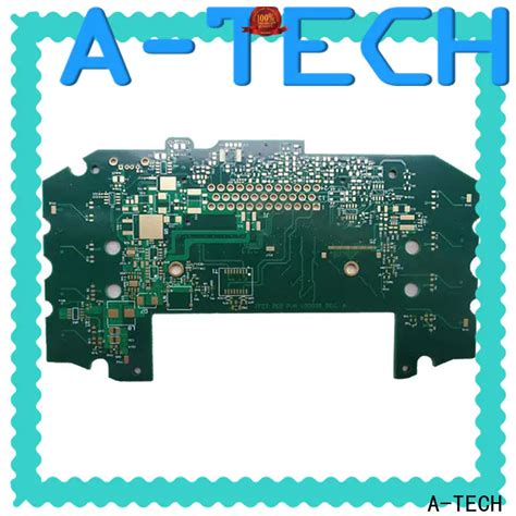
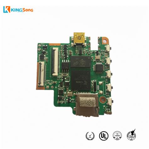
Printed wiring assembly (PWA) plays a vital role in modern electronic manufacturing, serving as the backbone of electronic device functionality. The process involves the assembly of printed circuit boards (PCBs), which are essential for establishing electrical connections between various components in a device. With the growing complexity of electronics, advancements in pcb assembly techniques have emerged, enhancing both the quality and efficiency of production. Traditional methods have evolved into more sophisticated practices, such as surface mount technology (SMT) and through-hole assembly. These innovative methods allow for higher component density and reduced footprints on PCBs.
Today’s pcba processes utilize automated machinery, which significantly reduces human error while increasing throughput. Moreover, new materials and coatings are introduced regularly, improving solderability and long-term durability. This shift not only leads to more reliable products but also fosters advancements in sustainability by minimizing waste during manufacturing. Below is a summary table highlighting key aspects of printed wiring assembly:
| Aspect | Traditional Techniques | Advanced Techniques |
|---|---|---|
| Labor Intensity | High | Low |
| Error Rate | Higher | Significantly Lower |
| Component Density | Moderate | High |
| Production Speed | Slower | Faster |
| Sustainability | Limited | Enhanced |
With the increasing demand for high-performance electronics across various industries, a deeper understanding of printed wiring assembly becomes crucial. As manufacturers embrace these advancements, they pave the way for innovative solutions that cater to both consumer needs and technological trends.
Historical Evolution of Printed Wiring Techniques
The journey of printed wiring assembly (PWA) can be traced back to the mid-20th century, when the demand for more efficient and compact electronic devices began to rise. Early methods relied heavily on manually connecting components on boards, a process that was not only labor-intensive but also prone to errors. As technology progressed, the introduction of printed circuit boards (PCBs) transformed the landscape of electronic manufacturing. This innovation allowed for a more streamlined approach, as components could now be soldered onto a single board rather than requiring extensive wiring. PCB assembly (PCBA) became the standard practice, significantly enhancing productivity and consistency in production.
With ongoing advancements in materials and techniques, manufacturers began exploring options such as surface mount technology (SMT) and through-hole technology. These methods permitted greater density and complexity in designs without sacrificing performance. As a result, modern electronic devices are smaller and more reliable than ever before. The evolution of these techniques not only resulted in improved functionality but also paved the way for innovations such as multi-layer PCBs that enable intricate circuit designs.
"Investing in newer technologies is key to staying competitive in today’s fast-paced electronics market."
This historical progression highlights just how crucial PWA has become in contemporary electronic manufacturing, setting the stage for even greater innovations and efficiencies that are shaping the future of electronic assembly. The continuous improvements represent a commitment to enhancing both cost-effectiveness and reliability, ensuring that manufacturers can meet the ever-growing demands of the industry and consumers alike.
Innovative Methods in Printed Wiring Assembly
The field of printed wiring assembly (PWA) has witnessed remarkable innovations that enhance the efficiency and accuracy of the pcb assembly process. One of the most prominent methods gaining traction is the adoption of automation through advanced robotic systems. These systems not only expedite the assembly process but also minimize the margin for human error, resulting in improved consistency across production runs. Furthermore, 3D printing technology is revolutionizing how components are integrated into pcba designs, allowing for intricate geometries and complex layouts that were previously challenging to achieve. This method significantly contributes to reducing material waste and costs during manufacturing.
Another innovative approach involves the utilization of high-density interconnects (HDI) that enable more compact designs with increased functionality. These interconnects are crucial for modern electronic devices that demand miniaturization without compromising on performance. The integration of smart manufacturing practices, including real-time monitoring and predictive maintenance, further optimizes the printed wiring assembly process, ensuring better resource allocation and minimizing downtime.
Moreover, leveraging advanced materials designed for better thermal conductivity and signal integrity plays a significant role in enhancing overall reliability in assembly techniques. The combination of these innovative methods not only streamlines production but also plays a crucial role in meeting the growing demands for high-performing electronic products in today’s market. Overall, these advancements signify a transformative era in pcb assembly, leading to higher quality outcomes with improved economic incentives for manufacturers.
Benefits of Advanced Assembly Techniques
The evolution of printed wiring assembly (PWA) techniques has brought about significant advantages, greatly enhancing the efficiency and reliability of pcb assembly processes. One of the key benefits of advanced pcba techniques is their ability to reduce production time significantly. This reduction is achieved through the implementation of automated systems and improved placement accuracy, allowing for faster manufacturing cycles and decreased labor costs. Furthermore, these innovative methods lead to a more compact design, helping to optimize space on printed circuit boards while accommodating more components without compromising performance. Enhanced printed wiring assembly processes also contribute to improved soldering quality, which further increases the overall reliability of electronic devices. The integration of advanced materials and technologies ensures optimal heat dissipation and electrical performance, reducing the likelihood of failures in harsh operating environments. In essence, adopting these cutting-edge assembly techniques not only streamlines manufacturing but also results in durable electronic products that can meet the increasing demands of modern technology.
Cost-Effectiveness in Modern Electronic Manufacturing
The landscape of modern electronic manufacturing has been significantly transformed by advancements in printed wiring assembly (PWA), particularly in terms of cost-effectiveness. As companies strive to optimize their production processes, PCB assembly has emerged as a critical component, facilitating the rapid and efficient creation of high-quality electronic devices. By leveraging innovative PCBA techniques, manufacturers can streamline their operations, reducing waste and minimizing overhead costs. Technologies such as automated assembly and surface mount technology (SMT) have not only enhanced productivity but also improved precision, leading to reduced error rates and lower rework costs. The integration of advanced materials and processes in pcb assembly further contributes to cost savings by increasing the lifespan and reliability of the products. Consequently, these advancements allow manufacturers to offer competitive pricing while maintaining high standards of quality. Ultimately, the cost-effectiveness derived from modern methods in printed wiring assembly plays a pivotal role in driving the growth and sustainability of the electronics manufacturing sector.
Enhancing Reliability through Improved Techniques
The reliability of pcb assembly is crucial in ensuring that electronic devices perform optimally and withstand various operating conditions. Recent advancements in printed wiring assembly techniques have significantly contributed to enhancing this reliability. By employing innovative methods such as the use of advanced materials and precision manufacturing processes, manufacturers can minimize defects and improve the overall durability of pcba products. Techniques like automated optical inspection (AOI) and X-ray inspection allow for thorough testing and verification at various stages of the assembly process, ensuring that each component is correctly placed and functioning as intended. Moreover, the integration of surface mount technology (SMT) has enabled much smaller components to be securely mounted on the printed circuit board, reducing the risk of mechanical failure. These improved techniques not only bolster endurance but also enhance cost-effectiveness, allowing manufacturers to deliver high-quality products in a competitive market. As these advancements continue to evolve, they play a vital role in meeting the increasing demands for reliability in today’s increasingly complex electronic systems.
Future Trends in Printed Wiring Assembly
As the electronic manufacturing industry continues to evolve, the future of printed wiring assembly (PWA) is set to become increasingly innovative and efficient. One of the most notable trends is the integration of automation and artificial intelligence within pcb assembly processes. This shift not only streamlines production but also enhances precision, drastically reducing the likelihood of errors associated with manual assembly. Furthermore, the rise of flexible and wearable electronics is driving new approaches to pcba, allowing manufacturers to create lightweight and adaptable circuits that can conform to various shapes and surfaces.
In addition to automation, advances in materials science are paving the way for more sophisticated substrates and components that improve performance and durability. The development of advanced materials enables manufacturers to produce assemblies that withstand harsh environments while maintaining reliable functionality. Additionally, sustainability is becoming a paramount consideration; thus, eco-friendly materials and processes are being prioritized in printed wiring assembly practices.
Moreover, with the growing demand for miniaturization in consumer electronics, techniques such as micro-manufacturing are at the forefront of pwa evolution. These methods allow for dense packing of components on smaller PCBs without compromising performance or reliability. Thus, as these trends unfold, businesses must adapt their strategies in order to remain competitive and meet customer expectations for more reliable, cost-effective solutions in the realm of modern electronic manufacturing.
Conclusion: The Impact of Advancements on the Industry
The advancements in printed wiring assembly (PWA) techniques have significantly transformed the pcb assembly landscape, enhancing not just production efficiency but also the overall quality of electronic products. With cutting-edge methods like selective soldering and automated optical inspection, manufacturers can reduce errors, resulting in a more reliable pcba (printed circuit board assembly). These innovations foster a more streamlined production process, pairing speed with precision and ultimately driving down costs. Moreover, as industries continue to demand higher performance and miniaturization of electronic components, such advancements ensure that manufacturers can meet these challenges while maintaining compliance with stringent quality standards. The ongoing evolution in pcb assembly technology doesn’t merely enhance manufacturing capabilities; it also paves the way for future generations of electronics that are not only efficient but also sustainable. Therefore, the impact of these advancements extends beyond immediate benefits, shaping the trajectory of the entire industry towards greater reliability and innovation.
Conclusion: The Impact of Advancements on the Industry
The evolution of printed wiring assembly (PWA) techniques has markedly transformed the landscape of electronic manufacturing. As we reflect on these advancements, it becomes evident that they have significantly bolstered the efficiency and cost-effectiveness of pcb assembly processes. Innovative methods such as automated machine placements and better soldering techniques have not only streamlined production but also enhanced the overall reliability of pcba products. This is paramount for industries where durability and performance are non-negotiable. Moreover, by integrating advanced technologies, manufacturers can reduce waste and optimize resource allocation, leading to a more sustainable production model. In essence, these developments not only cater to the immediate demands of electronic manufacturing but also pave the way for future innovations that will further reinforce the pivotal role of PWA in global markets. As such, it is clear that embracing modernized printed wiring assembly techniques is not merely an option; it has become a fundamental necessity for companies aiming to maintain competitiveness in an ever-evolving technological landscape.
FAQs
What is printed wiring assembly (PWA)?
Printed wiring assembly, commonly referred to as pcb assembly or pcba, is the process of assembling electronic components onto a printed circuit board (PCB). This technique is crucial for creating reliable electronic devices.
What are the benefits of using modern PWA techniques?
Modern pcb assembly techniques enhance efficiency, reduce production costs, and improve the overall reliability of electronic products. These advancements lead to faster production times and higher quality end-products.
How do innovations in PWA impact cost-effectiveness?
Innovations like automated assembly equipment and advanced inspection techniques lower labor costs and minimize errors during manufacturing. This increasing efficiency ultimately makes pcba processes more cost-effective.
What improvements have been made in reliability?
Through advanced assembly techniques, manufacturers can now achieve more precise component placement and better soldering quality. These improvements ensure that products are not only functional but also durable over time.
What are future trends in printed wiring assembly?
Future trends include the adoption of machine learning for process optimization and greater integration of environmentally sustainable materials in pcb assembly, aiming for both reliability and eco-friendliness.
For more information on advanced pcb assembly, please click here: Andwin PCB Assembly