Printed Circuit Boards (PCBs): The Foundation of Modern Electronics
Introduction
Printed Circuit Boards (PCBs) are the unsung heroes of modern electronics. They are the backbone of virtually every electronic device we use today, from smartphones and laptops to medical equipment and automotive systems. PCBs provide the mechanical support and electrical connections necessary for electronic components to function as intended. This article delves into the world of PCBs, exploring their history, design, manufacturing process, types, applications, and future trends. By the end of this article, you will have a comprehensive understanding of the critical role PCBs play in our daily lives and the technological advancements that continue to shape their evolution.
1. The History of PCBs
The concept of PCBs dates back to the early 20th century. In 1925, Charles Ducas patented a method for creating an electrical path directly on an insulated surface, which laid the groundwork for modern PCBs. However, it wasn’t until the 1940s and 1950s that PCBs began to gain widespread use, particularly in military applications during World War II. The need for reliable, compact electronics in military equipment drove the development of early PCB technology.
The 1950s and 1960s saw significant advancements in PCB technology. The introduction of double-sided boards allowed for more complex circuits, while multilayer PCBs revolutionized the industry by enabling higher component density. These innovations paved the way for the miniaturization of electronic devices, which became increasingly important as consumer electronics began to dominate the market.
2. PCB Design: Principles and Best Practices
The design of a PCB is a critical step in the development of any electronic device. It involves several stages, including schematic capture, component placement, routing, and verification.
- Schematic Capture: This is the initial stage where the electrical connections between components are defined using a schematic diagram. The schematic serves as a blueprint for the PCB layout. It is essential to ensure that the schematic is accurate and complete, as any errors at this stage can lead to significant issues later in the design process.
- Component Placement: Once the schematic is complete, the next step is to place the components on the PCB. This involves determining the optimal location for each component to ensure efficient routing and minimize signal interference. Factors such as thermal management, signal integrity, and mechanical constraints must be considered during component placement.
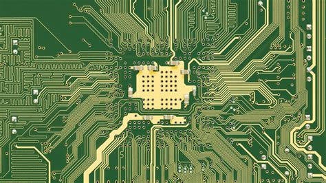
- Routing: Routing is the process of creating the conductive pathways (traces) that connect the components on the PCB. This can be done manually or using automated routing tools. The goal is to create a layout that minimizes signal loss, crosstalk, and electromagnetic interference (EMI). High-speed signals, in particular, require careful routing to maintain signal integrity.
- Verification: After the routing is complete, the design must be verified to ensure that it meets all electrical and mechanical requirements. This includes checking for design rule violations, signal integrity issues, and thermal performance. Design verification tools can help identify and resolve potential issues before the PCB is manufactured.
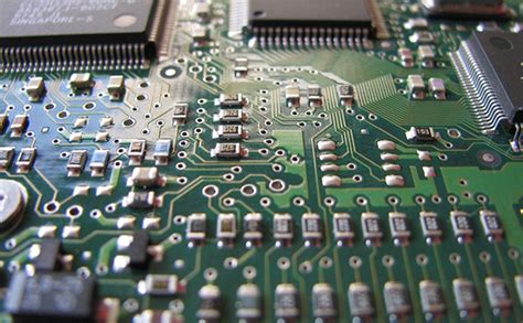
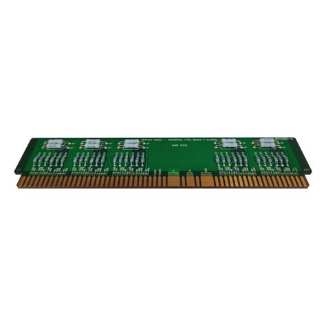
3. The PCB Manufacturing Process
The manufacturing of PCBs is a complex process that involves several steps, each of which must be carefully controlled to ensure the quality and reliability of the final product.
- Substrate Preparation: The process begins with the preparation of the substrate, which is typically made of fiberglass-reinforced epoxy resin (FR-4). The substrate is cut to the required size and cleaned to remove any contaminants.
- Copper Cladding: A thin layer of copper is then laminated onto the substrate. This copper layer will form the conductive traces of the PCB. The thickness of the copper layer can vary depending on the specific requirements of the PCB.
- Patterning: The next step is to create the desired circuit pattern on the copper-clad substrate. This is typically done using a photolithographic process, where a photoresist is applied to the copper, exposed to UV light through a mask, and then developed to remove the unexposed areas. The exposed copper is then etched away using a chemical solution, leaving behind the desired circuit pattern.
- Drilling: Holes are drilled into the PCB to accommodate through-hole components and vias (connections between layers in multilayer boards). The drilling process must be precise to ensure that the holes are properly aligned and sized.
- Plating: The drilled holes are plated with copper to create electrical connections between layers. This is typically done using an electroplating process, where a thin layer of copper is deposited onto the walls of the holes.
- Solder Mask Application: A solder mask is applied to the PCB to protect the copper traces from oxidation and to prevent solder bridges during assembly. The solder mask is typically green, but other colors are also available.
- Silkscreen Printing: Component labels and other identifying marks are printed onto the PCB using a silkscreen process. This helps with the assembly and troubleshooting of the PCB.
- Surface Finish: Finally, a surface finish is applied to the exposed copper to protect it from oxidation and to improve solderability. Common surface finishes include HASL (Hot Air Solder Leveling), ENIG (Electroless Nickel Immersion Gold), and OSP (Organic Solderability Preservative).
4. Types of PCBs
PCBs come in various types, each suited to different applications and design requirements.
- Single-Sided PCBs: These are the simplest type of PCBs, with components and traces on only one side of the substrate. They are typically used in low-cost, low-complexity applications.
- Double-Sided PCBs: These PCBs have components and traces on both sides of the substrate, allowing for more complex designs. They are commonly used in consumer electronics and industrial controls.
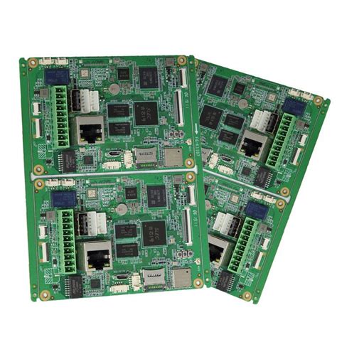
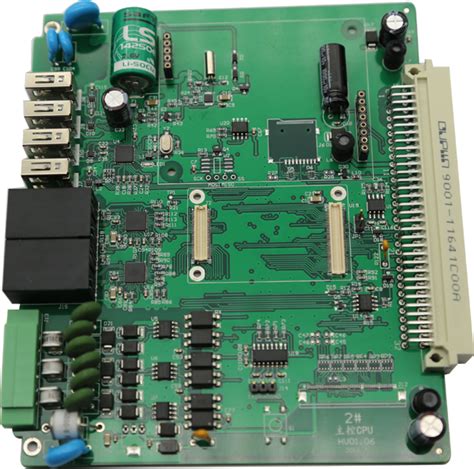
- Multilayer PCBs: Multilayer PCBs consist of multiple layers of substrate and copper, with connections between layers made through vias. They are used in high-density, high-performance applications such as smartphones, computers, and medical devices.
- Flexible PCBs: Flexible PCBs are made from flexible materials such as polyimide, allowing them to bend and conform to different shapes. They are used in applications where space and weight are critical, such as wearable devices and aerospace systems.
- Rigid-Flex PCBs: These PCBs combine the benefits of rigid and flexible PCBs, with rigid sections for component mounting and flexible sections for interconnections. They are used in complex applications such as military and medical equipment.
5. Applications of PCBs
PCBs are used in a wide range of applications across various industries.
- Consumer Electronics: PCBs are the backbone of consumer electronics such as smartphones, tablets, laptops, and televisions. They enable the compact and efficient design of these devices.
- Automotive: Modern vehicles rely on PCBs for various functions, including engine control, infotainment systems, and advanced driver-assistance systems (ADAS).
- Medical Devices: PCBs are used in medical devices such as pacemakers, imaging systems, and diagnostic equipment. They must meet stringent reliability and safety standards.
- Industrial Equipment: PCBs are used in industrial control systems, robotics, and automation equipment. They must be robust and reliable to withstand harsh industrial environments.
- Aerospace and Defense: PCBs are used in aerospace and defense applications, including avionics, communication systems, and radar. They must meet high reliability and performance standards.
6. Future Trends in PCB Technology
The PCB industry is continuously evolving, driven by advancements in technology and changing market demands.
- Miniaturization: As electronic devices become smaller and more compact, there is a growing demand for miniaturized PCBs with higher component density. This trend is driving the development of advanced manufacturing techniques and materials.
- High-Speed Design: The increasing demand for high-speed data transmission is driving the development of PCBs with improved signal integrity and reduced EMI. This includes the use of advanced materials and design techniques to minimize signal loss and crosstalk.
- Flexible and Stretchable PCBs: The development of flexible and stretchable PCBs is opening up new possibilities for wearable devices, medical implants, and other applications where traditional rigid PCBs are not suitable.
- Sustainability: There is a growing focus on sustainability in the PCB industry, with efforts to reduce the environmental impact of PCB manufacturing through the use of eco-friendly materials and processes.
- Advanced Materials: The use of advanced materials such as high-frequency laminates and thermally conductive substrates is enabling the development of PCBs with improved performance and reliability.
Conclusion
Printed Circuit Boards are an essential component of modern electronics, enabling the functionality of a wide range of devices across various industries. The design and manufacturing of PCBs involve a complex and highly controlled process, with continuous advancements in technology driving the development of more compact, high-performance, and sustainable PCBs. As the demand for electronic devices continues to grow, the importance of PCBs in enabling innovation and progress cannot be overstated. From their humble beginnings to their current state, PCBs have played a crucial role in the evolution of electronics, and they will continue to be at the heart of technological advancements in the future.