Noise reduction technology for DSP systems
With the emergence of high-speed DSPs (digital signal processors) and peripherals, new product designers are facing an increasingly serious threat of electromagnetic interference (EMI). In the early days, emission and interference issues were referred to as EMI or RFI (radio frequency interference). Now it is replaced by the more specific term “interference compatibility”. Electromagnetic compatibility (EMC) includes both emission and sensitivity issues of the system. If the interference cannot be completely eliminated, it must be minimized. If a DSP system meets the following three conditions, the system is electromagnetically compatible.
- No interference to other systems.
- Insensitive to the emission of other systems.
- No interference to the system itself.
Definition of interference
Interference is caused when the energy of the interference puts the receiver in an undesirable state. Interference is generated either directly (through conductors, common impedance coupling, etc.) or indirectly (through crosstalk or radiation coupling). Electromagnetic interference is generated through conductors and through radiation. Many electromagnetic emission sources, such as lighting, relays, DC motors and fluorescent lamps, can cause interference. AC power lines, interconnect cables, metallic cables, and subsystem internal circuits can also radiate or pick up unwanted signals. In high-speed digital circuits, clock circuits are often the largest source of broadband noise. In fast DSPs, these circuits can generate harmonic distortion up to 300MHz and should be removed from the system. In digital circuits, the most susceptible are reset, interrupt, and control lines.
Conducted EMI
One of the most obvious, but often overlooked, paths that can cause noise in a circuit is through conductors. A wire passing through a noisy environment can pick up noise and send it to another circuit causing interference. Designers must avoid wires picking up noise and use decoupling to remove noise before it causes interference. The most common example is noise entering a circuit through power lines. If the power supply itself or other circuits connected to the power supply are the source of interference, the power supply line must be decoupled before it enters the circuit.

Common impedance coupling
Common impedance coupling occurs when currents from two different circuits flow through a common impedance. The voltage drop across the impedance is determined by the two circuits. The ground currents from the two circuits flow through the common ground impedance. The ground potential of circuit 1 is modulated by ground current 2. Noise signals or DC offsets are coupled from circuit 2 to circuit 1 via the common ground impedance.
Radiated Coupling
Coupling via radiation is commonly known as crosstalk, which occurs when current flows through a conductor and generates an electromagnetic field that induces transient currents in adjacent conductors.
Radiated Emissions
There are two basic types of radiated emissions: differential mode (DM) and common mode (CM). Common mode radiation, or monopole antenna radiation, is caused by an unintentional voltage drop that raises all ground connections in the circuit above the system ground potential. CM radiation is a more serious problem than DM radiation in terms of electric field magnitude. To minimize CM radiation, common mode currents must be reduced to zero with practical designs.
Factors Affecting EMC
Voltage – Higher supply voltage means higher voltage amplitudes and more emissions, while lower supply voltages affect sensitivity.
Frequency – High frequencies produce more emissions, and periodic signals produce more emissions. In high-frequency digital systems, current spikes are generated when devices switch; in analog systems, current spikes are generated when the load current changes.
Grounding – Nothing is more important to circuit design than a reliable and perfect power system. Of all EMC problems, the main problem is caused by improper grounding. There are three signal grounding methods: single point, multi-point and mixed. Single-point grounding can be used at frequencies below 1MHz, but it is not suitable for high frequencies. In high-frequency applications, multi-point grounding is best used. Mixed grounding is a method of using single-point grounding for low frequencies and multi-point grounding for high frequencies. Ground layout is critical. The ground loops of high-frequency digital circuits and low-level analog circuits must never be mixed.
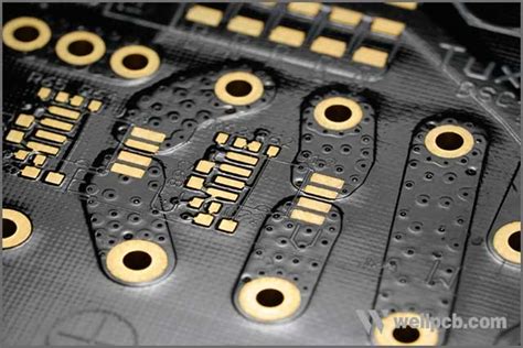
PCB design – Proper printed circuit board (PCB) routing is crucial to preventing EMI.
Power supply decoupling – When devices switch, transient currents are generated on the power supply line, which must be attenuated and filtered out. Transient currents from high di/dt sources cause ground and trace “shooting” voltages. High di/dt generates large-scale high-frequency currents, exciting components and cables to radiate. The change in current and inductance flowing through the wire will cause a voltage drop. Reducing the inductance or the change in current over time can minimize the voltage drop.
Technology to reduce noise
There are three ways to prevent interference:
- Suppress source emission.
- Make the coupling path as ineffective as possible.
- Make the receiver as sensitive to emission as possible.
The following introduces board-level noise reduction technology. Board-level noise reduction technology includes board structure, line arrangement and filtering.
Board construction noise reduction techniques include:
- Use ground and power planes
- Make planes large to provide low impedance for power decoupling
- Minimize surface conductors
- Use narrow traces (4 to 8 mils) to increase high-frequency damping and reduce capacitive coupling
- Separate digital, analog, receiver, transmitter ground/power lines
- Separate circuits on the PCB by frequency and type
- Do not score the PCB; traces near scorelines may cause unwanted loops
- Use multi-layer boards to seal traces between power and ground layers
- Avoid large open-loop board layer structures
- Connect PCB connectors to chassis ground, which provides shielding to prevent radiation at circuit boundaries
- Use multi-point grounding to keep high-frequency ground impedance low
- Keep ground pins shorter than 1/20 of the wavelength to prevent radiation and ensure low impedance line arrangement noise reduction techniques include using 45. Instead of 90. Trace turns, 90. Turns increase capacitance and cause changes in the characteristic impedance of the transmission line
- Keep the spacing between adjacent excitation traces greater than the width of the trace to minimize crosstalk
- Keep the clock signal loop area as small as possible
- Keep high-speed lines and clock signal lines short and directly connected
- Do not run sensitive traces parallel to traces that carry high-current fast switching transitions
- Do not have floating digital inputs to prevent unnecessary switching transitions and noise generation
- Avoid power supply traces under crystals and other inherently noisy circuits
- Run corresponding power, ground, signal and return traces in parallel to eliminate noise
- Keep clock lines, bus lines and chip enables separated from input/output lines and connectors
- Route clock signals orthogonal to I/O signals
- To minimize crosstalk, use right-angle crossings and interspersed ground lines
- Protect critical traces (use 4 mil to 8 mil traces to minimize inductance, route close to the floor layer, sandwich structure between board layers, and protect each side of the sandwich with ground)
Filtering techniques include:
- Filter the power lines and all signals entering the PCB
- Decouple the original pins at each point of the IC with high-frequency low-inductance ceramic capacitors (0.1UF for 14MHz and 0.01UF for more than 15MHz)
- Bypass all power supply and reference voltage pins of the analog circuit
- Bypass fast switching devices
- Decouple the power supply/ground at the device leads
- Use multi-stage filtering to attenuate multi-band power supply noise
Other noise reduction design techniques include:
- Install the crystal oscillator embedded in the board and ground it
- Add shielding in appropriate places
- Use series terminals to minimize resonance and transmission reflections. Impedance mismatch between the load and the line will cause partial reflection of the signal. Reflection includes transient disturbances and overshoots, which will generate large EMI
- Arrange adjacent ground lines close to signal lines to more effectively prevent the appearance of electric fields
- Properly place the decoupling line driver and receiver close to the actual I/O interface, which can reduce coupling to other circuits on the PCB and reduce radiation and sensitivity
- Shield and twist the interfering leads together to eliminate mutual coupling on the PCB
- Use clamping diodes on inductive loads
EMC is an important issue to be considered in DSP system design. Appropriate noise reduction technology should be used to make the DSP system meet EMC requirements