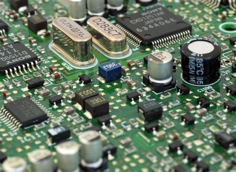
Dry film solder mask for printed circuit boards
Dry film solder mask is not in liquid or paste form, it appears in the form of a photosensitive polymer film, which is sandwiched between two protective layers. These two protective layers protect the middle photosensitive emulsion film to prevent it from being damaged during operation. The steps for applying dry film solder mask are detailed as follows:
1.Surface preparation
At this stage, the tin/tin-lead metal solder mask on the circuit board surface is stripped and the circuit board surface is cleaned with clean water and thoroughly dried, and then the copper surface is subjected to a series of cleaning processes, such as:
1) Degrease with hot strong alkaline solution;
2) Water rinse;
3) Micro-etching of the surface copper layer by 1-2.5μm, which is to enhance the adhesion of the dry photosensitive polymer film to the surface;
4) Inspection to ensure complete removal of tin/tin-lead;
5) Water rinse;
6) Dip in 10% sulfuric acid for 1-2min.
7) Water rinse;
8) Abrasive cleaning (320 abrasive brush and pumice scrub)
9) High pressure water rinse and drying. Controlled oxidation of the copper layer with brown oxide and black oxide is used to increase the adhesion between the surface and the solder mask. The oxidation process must be strictly controlled to keep the oxide layer thickness at 0.5-1.0μm. If the oxidized circuit board is stored for too long, the surface must be thoroughly degreased before lamination.
2.Pre-lamination drying
The absorption of moisture and water residue are the most common causes of blistering and delamination of circuit boards. Therefore, it is particularly important to remove all the standing water from the surface and holes of the printed circuit board. A high-pressure hair dryer can be used to physically remove water from the surface and holes of the circuit board. A high-pressure vacuum air knife can also be used in this step.
The absorbed moisture of the circuit board can be removed by baking the circuit board at (1 10±10) “C for 15-20min, or by using an infrared oven equipped with a conveyor belt at 80-120 “C for 30s. Different substrates and different thicknesses of circuit boards require different drying times. Excessive baking time and baking temperature should be avoided because this will increase the formation of copper oxides and lead to poor adhesion.

3.Lamination
Vacuum lamination ensures that all wires are completely encapsulated by the photosensitive polymer solder mask and that there are no residual bubbles on the circuit board.
4.Selection of mask width
The selection of dry film width should be based on the width of the process board. The width of the dry film should not exceed 10 mm of the process board width to avoid edge trimming loss. Lamination can be done on both sides at the same time or on one side first and then on the other side, which is mainly determined by the type of laminator used and the type of dry film.
5.Holding time after lamination
The holding time between lamination and exposure should be carefully controlled to achieve the best results. When lamination is just completed, the required exposure energy is low, which increases rapidly with the increase of holding time and gradually stabilizes to a constant value. Therefore, the holding time after lamination should be kept at a constant value to avoid drastic changes in exposure time.
6.Exposure (film)
Usually, photopolymer solder mask works negatively, so it requires a positive film (opaque pad area) for exposure. Due to the high energy required, the film must have a very high density, and its maximum density Dmax must be greater than 4 to avoid solder mask in the pad area, and the minimum density Dmin of the blank area must be less than 0.15. Since the density of the mask changes with use, the film must be checked periodically to ensure that the minimum Dmax is greater than 4.
Usually, the best effect can be obtained by using a 7mil single-sided film azo brown film. For alignment systems that do not require alignment through the pad, a silver halide mask can be used, and its filmed side can be tightly attached to the circuit board to obtain the best exposure effect and realistic edge straightness. The minimum opaque pad area of the film should be 0.1-0.15mm, which should be slightly larger than the diameter of the pad on the printed circuit board.
By using the Stouffer 21-step exposure ruler Θ, the exposure time and subsequent polymerization degree can be determined and monitored. In order to determine the correct exposure value, the holding time and the developing conditions must be compatible. The Stouffer 21-step exposure ruler used defines more than 50% solder resist coverage as the last stage. A certain compatible holding time is required to allow the polymerization process to complete and enter a stable state.
7.Development
The development process is to wash away the unexposed (unpolymerized) solder resist from the surface of the printed circuit board. The development time of a specific type of photosensitive polymer depends on the chemical used. The correct development time is determined by controlling the time point at which the unexposed resist can be completely washed away from the surface of the printed circuit board. The solder resist needs to be completely removed from the pads and holes of the circuit board to obtain good solderability. Commonly used chemicals are: aqueous solution and developer.
In aqueous development, a diluted uranium carbonate solution is usually added to 99% pure water at a temperature of 45 ‘C. After using this solution, the flushing distance of the printed circuit board during full development should be between 40% and 60% of the length of the development chamber. When using a developer, 1-1-1 trichloroethane is used, and the development point should be set at 25% of the total length of the development chamber.
8.Drying
In order to obtain satisfactory curing results, the board must be thoroughly dried after development. By using a hot air knife to heat the circuit board at 90 ‘t for 15 minutes, the moisture absorbed by the solder mask and substrate on the circuit board during the development and cleaning stages can be completely removed.
9.Curing
In order to achieve optimal soldering performance and prevent mask warping during wave soldering and vapor phase soldering, the photosensitive polymer resist must be properly cured.
Ultraviolet (UV) curing of photopolymer solder mask can be accomplished using conventional curing equipment using soft gas lamps. The required energy level is achieved by controlling the density of the soft gas lamps and the speed of the conveyor belt. It is best to absorb enough energy to completely agglomerate one side of the board in one pass. The UV lamp should use a 200W/in high pressure mercury vapor lamp. Since the heat emitted by the UV lamp is an integral part of the curing process, it is not recommended to use a “cool” UV unit to reduce the amount of heat reaching the board. Surface temperatures of the board less than 105°C during the UV curing process often result in poor curing results. Attention should also be paid to not overheat the board during the UV curing process. The typical temperature should be between 110-140°C. Excessive heating will cause the photopolymer to become brittle and blistering to occur on the surface.
During the heat curing process, the temperature of the oven used to bake the board should be completely uniform throughout the oven chamber. These ovens should not be used for other purposes to prevent contamination of the solder mask. Ovens without fresh air inlet should not be used because the hot air may condense on the board surface and reduce solderability. In addition, if the air in the oven is not diluted, the hot air will reach a dangerous temperature that may explode. For the oven to work safely, a thermostatic timer and temperature recorder should be provided. An exhaust fan is also required to spread the heat throughout the oven chamber. The oven chamber should also be equipped with an exhaust duct with a blower.
Dry film solder mask manufactured under certain controlled conditions has a uniform thickness. When applying this mask, a high pressure laminator is used to ensure uniform coating of the entire process board area. This method can also maintain uniform coating of process boards from different batches and heats.
Both screen printing and curtain coating processes are single-sided processing systems. In other words, the application of solder mask can only be done on one side at a time. The board must be dried to remove the ink glue adhesive before printing the other side, which makes the second side processing also take a long time. Using a vacuum laminator, dry film solder mask can be applied to both sides of the board at the same time.