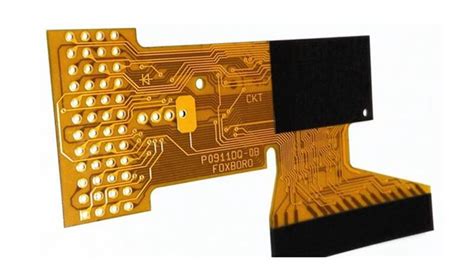
Principle of Single In-line Package (SIP)
In a single in-line package (SIP), the pins are led out from one side of the package and arranged in a straight line. Usually, they are through-hole type, and the pins are inserted into the metal holes of the printed circuit board. When assembled on the printed circuit board, the package is sideways. A variation of this form is the zigzag single in-line package (ZIP), whose pins still extend from one side of the package body, but are arranged in a zigzag shape. In this way, the pin density is increased within a given length range. The pin center distance is usually 2.54mm, and the number of pins ranges from 2 to 23, most of which are customized products. The shape of the package varies. Some also call the package with the same shape as ZIP SIP.
SIP packaging has no fixed form.
In terms of chip arrangement, SIP can be a planar 2D package of a multi-chip module (MCM), or it can use a 3D package structure to effectively reduce the package area; and its internal bonding technology can be simple wire bonding (Wire Bonding), or it can use flip chip bonding (Flip Chip), but it can also be a mixture of the two. In addition to 2D and 3D packaging structures, another way to integrate components with a multifunctional substrate can also be included in the scope of SIP. This technology mainly hides different components in a multifunctional substrate, which can also be regarded as the concept of SIP to achieve the purpose of functional integration.
Different chip arrangements, combined with different internal bonding technologies, make SIP packaging types produce a variety of combinations, and can be customized or flexibly produced according to customer or product needs.
The elements that constitute SIP technology are packaging carriers and assembly processes.
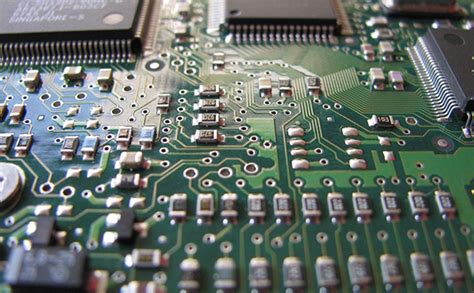
The former includes PCB, LTCC, Silicon Submount (which can also be an IC itself). The latter includes traditional packaging processes (Wirebond and Flip Chip) and SMT equipment. Passive components are an important part of SIP, some of which can be integrated with the carrier (Embedded, MCM-D, etc.), and others (high-precision, high-Q, high-value inductors, capacitors, etc.) are assembled on the carrier through SMT. The mainstream packaging form of SIP is BGA. Judging from the current technical situation, SIP itself has no special process or materials.
This does not mean that having traditional advanced packaging technology means mastering SIP technology.
Since the industrial model of SIP is no longer a single foundry, module division and circuit design are other important factors.
Module division refers to separating a piece of function from an electronic device, which is convenient for subsequent whole-machine integration and SIP packaging. Circuit design should consider the details inside the module, the relationship between the module and the outside, and the integrity of the signal (delay, distribution, noise, etc.). With the increase of module complexity and the increase of operating frequency (clock frequency or carrier frequency), the difficulty of system design will continue to increase, resulting in multiple iterations of product development and rising costs. In addition to design experience, numerical simulation of system performance must participate in the design process.
Compared with system integration on printed circuit boards, SIP can maximize system performance, avoid repeated packaging, shorten development cycles, reduce costs, and improve integration.
Compared with SoC, SIP has the characteristics of high flexibility, high integration, short design cycle, low development cost, and easy entry. SIP will break the current industrial structure of integrated circuits and change the situation where packaging is just a back-end processing plant. In the future, a group of entities that combine design capabilities and packaging processes will appear in the integrated circuit industry, mastering their own brand products and profits.
At present, the output value of packaging in the world only accounts for 10% of the total value of integrated circuits.
When SIP technology is mastered by packaging companies, the industrial structure will begin to adjust, and the output value of the packaging industry will increase by leaps and bounds.
SIP packaging can integrate other components required by the system such as passive components and antennas into a single package, making it more complete system functions. From the perspective of application products, SIP is more suitable for electronic products with low cost, small area, high frequency and high speed, and short production cycle, especially in the portable product market such as power amplifiers (PA), global positioning systems, Bluetooth modules (Bluetooth), image sensor modules, memory cards, etc. However, in many systems, closed circuit boards limit the height and application of SIP. In terms of long-term development planning, the development of SoC will effectively improve the performance requirements of future electronic products, and the packaging type it is suitable for will also be based on flip chip technology that can provide better performance; compared with the development of SoC, SIP will be more suitable for cost-sensitive communications and consumer product markets.
SIP technology can be applied to various fields of the information industry, but the most distinctive research and application at present is the physical layer circuit in wireless communication. Commercial RF chips are difficult to implement using silicon planar technology, which makes the integration that SoC technology can achieve relatively low and the performance is difficult to meet the requirements. At the same time, due to the high operating frequency of the physical layer circuit, various matching and filtering networks contain a large number of passive devices, and the technical advantages of SIP are fully demonstrated in these aspects. At present, SIP technology is still in its early stages.
Although a large number of products use SIP technology, the technical content of its packaging is not high. The system structure is similar to the system integration on PCB. It is nothing more than using unpackaged chips to combine with passive devices through COB technology. Most passive devices in the system are not integrated into the carrier, but SMT discrete devices.
Before the term SIP became popular, there were many products integrated in a single package.
Historical reasons have caused these products to not be labeled SIP so far. The earliest module was the power amplifier in the mobile phone. This type of module can integrate multi-frequency power amplifier, power control, and transceiver conversion switch. In addition, the integration of three-dimensional multi-chip storage modules and logic circuits and storage circuits is also in this situation.
Bluetooth and 802.11 (b/g/a) have a higher degree of integration.
In addition to the antenna, Philips’ BGB202 Bluetooth SIP module contains a baseband processor and all physical layer circuits, and part of the filter circuit is implemented using thin film technology (but not in the SIP carrier, but in the form of a discrete passive chip). The outer dimensions of the entire module are 7mm×8mm×1.4mm. The external unit only needs an antenna and a clock. Philips also has a mobile TV solution for 3G communications that also uses SIP technology. The 9mmx9mm module includes a high-frequency head, channel demodulation and decoding.
UWB is another ideal application for SIP. Freescale Semiconductor has begun to provide DS-UWB chipsets.