Analysis of the role of copper plating in PCB
- Reasons for copper plating:
EMC, copper plating for large areas of ground or power supply will play a shielding role, and some special grounds, such as PGND, play a protective role. - PCB process requirements, generally in order to ensure the electroplating effect, or lamination without deformation, copper is plating for PCB layers with less wiring.
- Signal integrity requirements, give high-frequency digital signals a complete return path, and reduce the wiring of the DC network. Of course, there are also heat dissipation, special device installation requires copper plating and other reasons.
- Benefits of copper plating
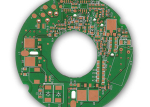
The biggest benefit of copper plating is to reduce ground impedance (the so-called anti-interference is also largely caused by the reduction of ground impedance). There are a lot of spike pulse currents in digital circuits, so it is more necessary to reduce ground impedance. It is generally believed that for circuits composed entirely of digital devices, large areas should be laid, while for analog circuits, the ground loop formed by copper plating will cause electromagnetic coupling interference, which is not worth the loss (except for high-frequency circuits). Therefore, not all circuits need copper (BTW: mesh copper is better than whole block copper)
The significance of copper is:
The copper is connected to the ground wire, which can reduce the loop area.
Large area copper is equivalent to reducing the resistance of the ground wire and reducing the voltage drop. From these two points of view, both digital ground and analog ground should be coppered to increase the anti-interference ability, and at high frequencies, the digital ground and analog ground should be separated and coppered, and then connected with a single point. The single point can be connected by winding a wire around a magnetic ring several times. However, if the frequency is not too high, or the working conditions of the instrument are not bad, it can be relatively relaxed. The crystal oscillator can be regarded as a high-frequency emission source in the circuit. You can lay copper around it and then ground the shell of the crystal oscillator, which will be better.

