Demystifying FPGAs for Software Engineers
As product designs grow in complexity, integrated components such as ASSPs are needed to meet design requirements. Years ago, engineers would select individual components for processors, memory, and peripherals, then piece these elements together using discrete logic devices. Later, they would search catalogs of ASSP processing systems, trying to find the best combination to meet system requirements. When they needed additional logic or peripherals, they would typically pair an FPGA with an ASSP to complete the solution. Indeed, surveys show that FPGAs are used in 50% to 70% of all embedded systems today.
Over the past few years, FPGAs have increased in size, providing enough space to house complete processor and logic systems in a single device. Now, software engineers need to develop and debug code for the processor inside the FPGA. In some cases, they dread doing so. However, mastering FPGA basics and understanding how to create and debug code for FPGA embedded processors can help them face the challenge.
What is an FPGA?
A field-programmable gate array (FPGA) is an integrated circuit that contains logic that can be configured and connected after manufacturing (i.e., “field mode”). In this regard, while engineers used to buy various logic devices from a product catalog and assemble them into a logic design through connections on a printed circuit board, hardware designers can now implement a complete design in a single device. In its simplest form, an FGPA includes:
● Configurable logic blocks consisting of AND, OR, NOT, and many other logic functions
● Configurable interconnect functions that allow logic blocks to be connected together
● I/O interfaces
With these elements, users can create arbitrary logic designs.
Hardware engineers usually write code in HDL (usually Verilog or VHDL), and then assemble the design into an object file that can be loaded into the device for execution. On the surface, an HDL program may look a lot like a high-level language such as C.

Technical advantages of FPGAs
Because ASICs are not used and there is no high template cost associated with them, FPGAs are the most flexible and cost-effective way to implement data processing elements. FPGAs, because of their flexible architecture, allow hardware designers to implement processing systems that contain both parallel and serial elements. This allows designers to optimize the system for performance and latency. These data processing systems typically achieve higher levels of performance than can be achieved using general-purpose processors, but at a lower cost.
You can couple an external microprocessor to a data processing system in an FPGA and use it for control. However, embedding a processor in the FPGA offers several advantages. An internal processor can greatly reduce latency between the processor and the data processing system, eliminating a significant number of processor cycles.
The communication channel between the processor and the data processing system can be 32 bits or higher, with more addressing and control wires. For an external processor, these additional wires may require a larger package to accommodate the processor and FPGA, driving up system cost. Alternatively, PCI Express (PCIe) can be used to reduce the number of pins. Unfortunately, because it is a relatively new interface, not all processors and FPGAs support PCIe. While PCIe has inherently high performance, it is a serial interface, which increases latency between the processor and the data processing system.
Implementing both the processor and data processing elements in an FPGA reduces component count, board space, and sometimes power consumption.
This can result in a significantly lower cost solution. FPGAs are available with either hardened processor implementations (such as the ARM Cortex-A9 processor) or soft core implementations (such as the Xilinx MicroBlaze processor). FPGA-based processors can also be configured based on the application’s requirements. FPGA-based systems allow for system-level tuning: it provides the flexibility to choose whether computational functions are implemented in the processor or in the FPGA logic.
Implementation Techniques
There are many ways to implement an FPGA embedded processing system, but they can generally be divided into three categories: assembling the system from scratch, using a wizard to put it together, or by modifying an existing design.
FPGA tools allow you to assemble a processing system from scratch by selecting the required IP from a list and then connecting the IP through buses and cables. While this assembly is effective, it can be time-consuming.
To speed things up, FPGA tools also allow for quick assembly of microprocessor systems through wizards. The target part and the required processor and peripherals can be easily specified using drop-down lists or check boxes. Figure 1 shows the introduction window that the wizard starts with and the final system generated by the wizard. Similarly, tools such as MATLAB? software can be used to quickly assemble a data processing system with a processor bus interface for control. Then, simply match the bus interface to connect the processor to the data processing system.
A third approach to implementing an embedded processing system is to modify an existing reference design or add it to an existing hard processor system. FPGA reference designs and hard processor systems continue to evolve, with many becoming more market-focused. In many cases, the designs are so comprehensive that the hardware designer does not need to add any additional components. Software designers often find complete drivers and operating systems prebuilt for these reference designs.
The first two approaches mentioned above are both valid ways to create a processor system. However, the third approach starts with an existing, proven reference design, so it can significantly reduce development time for both hardware and software engineers.
Clarifying Myths
Some myths have arisen in the engineering community about the difficulty of developing processor code in FPGAs. We hope to clarify these myths.
Myth: Writing code for processors in FPGAs is difficult.
Fact: Most FPGA embedded processing development is done in C or C++ in a modern software development environment.
Many FPGA vendors now support software development using Eclipse. Eclipse is a flexible, plug-in-enabled software development environment that provides text editors, compilers, linkers, debuggers, trace modules, and code management.
As an open environment, Eclipse has a large developer community that is constantly adding new features. For example, if a programmer doesn’t like the provided editor, they can install one that better suits their needs.
Myth: FPGAs don’t have processor systems like ASSPs.
Fact: There are pre-built FPGA soft embedded processor designs, as well as hard processor designs with peripheral sets like ASSPs.
FPGAs that include both soft and hard processors add an extra capability. The FPGA Embedded Soft Processor Reference Design combines a 32-bit RISC processor, memory interfaces, and industry-standard peripherals. The flexible nature of this type of processor allows users to trade logic for additional performance features, such as adding an MMU to support the latest operating systems. The wide selection of FPGAs allows users to select a processor configuration, peripherals, data processing logic, and logic performance level to meet their system requirements. Pre-built ASSP-like reference designs allow software designers to start writing code immediately without having to implement a processor system by a hardware engineer. In many cases, the pre-built design will meet the requirements of the embedded processor system, eliminating the need for a hardware engineer to perform further processor system design. In a few cases, the hardware engineer has an excellent platform to which they can add peripherals and connect custom hardware accelerators.
Myth: Debugging code with a processor in an FPGA is difficult.
Fact: Software debugging for FPGA embedded processors is as easy as debugging for non-embedded processors. Debuggers support downloading code, running programs, single-stepping at the source and object code levels, setting breakpoints, and inspecting memory and registers. In addition, there are other tools for characterizing and tracing code.
Myth: My favorite operating system is not supported.
Fact: Most common embedded processors support the most common operating systems, and the list is growing. Xilinx MicroBlaze supports Linux, ThreadX, MicroC/OS-II, and eCos.
Myth: There are no drivers.
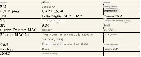
Fact: FPGA embedded processors have a large library of peripherals that include drivers. Table 1 is a representative list of some of the soft peripherals available for FPGA soft processors. Drivers exist for all of these devices.
Myth: The hardware engineer has to build it before I can write code.
Fact: Pre-built, tested processor system designs are available so software development can begin immediately.
These pre-built ASSP-like processor systems include the processor, memory controller and memory, flash controller, and peripherals such as UART, GPIO, and Ethernet interfaces. These systems are delivered with reference software design examples that include demonstration of Linux booting.
Myth: It is not possible to profile or trace with FPGA embedded processors.
Fact: Profiler and trace tools are available. Profiler allows developers to understand how much time the processor spends in various functions and how many times any given function is called.
Myth: FPGA software development tools are too expensive.
Fact: ASSP and FPGA vendors offer pricing between $200 and $500 for their embedded software development capabilities. In addition, many vendors offer trial versions and free or limited-feature versions, as well as discounted evaluation kits.
Create and debug code
The software development process for FPGA embedded processor systems follows some general steps:
● Create a software development workspace and import the hardware platform.
● Create a software project and board support package.
● Create the software.
● Run and debug the software project.
Optional step: Characterize the software project.
Steps 3, 4, and 5 are familiar to most developers. Some developers may not be familiar with steps 1 and 2, but these steps are clear. We will use the Eclipse development environment as an example to understand each step in more detail.
Create a workspace and import a hardware platform
After launching Eclipse, the user is prompted for the workspace to use. A workspace is a directory path that stores project files. Next, the user specifies the hardware platform (design). The hardware development tool automatically generates this file. This file describes the processor system, including memory interfaces and peripherals, and memory mapping. This file is the output of the hardware development tools and is usually provided by the hardware engineer to the software developer. Once specified, the hardware platform is imported and this step is complete.
Create Software Project and Board Support Package
A board support package (BSP) contains libraries and drivers for use by software applications. A software project is the software application source and settings.
In the version of Eclipse customized for Xilinx projects, you can select “File” → “New” → “Xilinx C Project”. For Xilinx C projects, Eclipse automatically creates Makefiles, compiles source files into object files, and links these object files into an executable file. In this step, the user can define the “Project Name”, associate it with the hardware platform by providing the hardware platform name created in step 1, and then specify the project name.
Next, the system confirms the generation of the BSP and automatically loads the applicable drivers based on the defined hardware platform and operating system. These drivers are then compiled to generate the BSP.
Creating Software
At this point you can import a software example, or create code from scratch. When you save your code, Eclipse automatically compiles and links it, and reports any compiler or linker errors that occur.
Running and Debugging Your Software Project
When working with FPGAs, there is one step that must be completed before you can execute your code: programming the FPGA. In Eclipse, simply select Tools → Program FPGA. This step takes the hardware design that your hardware engineer has created and downloads it to the FPGA. Once that job is complete, you can choose the type of software you want to build. Debug disables code optimization and inserts debug symbols, while Release enables code optimization. For profiling, use the -pg compile option.
Finally, you can run your code by selecting Run and defining the type of run configuration and compiler options. If Release is selected, the processor will immediately begin executing your code. Otherwise, the processor will execute some boot instructions and will stop at the first line of the source code, and the debug view will appear in Eclipse.
The debug view displays source or object code, registers, memory, and variables. You can step through the code at the source or object code level, and you can set breakpoints in the code execution.
Profiling a Software Project
If you want, you can profile the code at this point to see the number of function calls and the percentage of time spent in any given function. Figure 3 shows an example of an Eclipse profiling view with the profiler results.
Advantages of FPGAs
FPGA embedded processors are becoming a major design choice in terms of cost, power consumption, size, and overall system efficiency. The good news is that software engineers do not need to view FPGA embedded processors as mysterious or more difficult to program than external processors.
FPGA vendors provide industry-standard development environments (such as Eclipse) that are competitive in cost and customized for FPGA embedded processing. In these environments, users can create, compile, link, and download code, and debug their designs in the same way as they did with external processors. With pre-built processor reference designs, software engineers can start writing code and testing immediately without necessarily needing a hardware engineer to provide a final design. Finally, FPGA embedded processors have rich IP libraries, drivers, and operating system support.