Precision PCB Manufacturing Solutions by Invotec Europe
Key Takeaways
When exploring PCB manufacturing solutions, understanding the balance between advanced technologies, cost-efficiency, and reliability is critical. Invotec Europe stands out among PCB manufacturing companies by prioritizing a zero-defect philosophy, ensuring every circuit board meets stringent quality benchmarks. Their expertise in design for manufacturability (DFM) simplifies complex projects, translating concepts into functional designs while minimizing PCB manufacturing cost through optimized material usage and process efficiency.
Tip: Early collaboration with your PCB partner during the design phase can reduce revisions and accelerate time-to-market.
For industries requiring tailored solutions—such as aerospace, automotive, or medical devices—Invotec’s tailored manufacturing expertise addresses unique challenges, from multilayer integration to thermal management. Their end-to-end support covers prototyping to large-scale production, ensuring scalability without compromising precision. By leveraging advanced materials like high-frequency laminates and embedded components, they deliver high-performance PCBs capable of meeting Europe’s evolving technological demands.
A key advantage in the PCB manufacturing business lies in overcoming compatibility hurdles, particularly in multilayer designs. Invotec’s rigorous testing protocols and automated inspection systems ensure seamless integration, reducing the risk of field failures. Whether optimizing PCB manufacturing cost for startups or ensuring compliance with industry-specific standards, their solutions emphasize long-term reliability and innovation.
“Partnering with a trusted manufacturer transforms technical challenges into competitive advantages.”
By aligning with Invotec Europe, you gain a partner committed to navigating complexities in PCB manufacturing, from material selection to final validation. Their focus on zero-defect outcomes and customer-centric workflows positions them as a strategic resource for businesses aiming to excel in fast-paced, technology-driven markets.
Precision PCB Manufacturing: Meeting Europe’s Advanced Technology Demands
To meet Europe’s rapidly evolving technological needs, precision PCB manufacturing requires a blend of innovation, expertise, and rigorous quality control. As industries such as automotive, aerospace, and medical devices demand increasingly complex circuitry, partnering with leading PCB manufacturing companies becomes critical to ensuring performance and reliability. Invotec Europe addresses these challenges by integrating advanced design-for-manufacturability (DFM) principles, which streamline the transition from concept to production while minimizing PCB manufacturing cost and time-to-market. Their approach emphasizes optimizing layouts for scalability, reducing material waste, and leveraging cutting-edge fabrication technologies like high-density interconnect (HDI) and automated optical inspection (AOI).
A key differentiator lies in their ability to balance cost-efficiency with uncompromising quality—a necessity in sectors where even minor defects can lead to significant operational risks. By adopting a zero-defect philosophy, they ensure every layer of multilayer PCBs meets stringent reliability standards, whether for high-frequency applications or miniaturized designs. This focus on precision is further enhanced by their use of advanced materials, including low-loss substrates and thermal management solutions, which cater to Europe’s push for energy-efficient and durable electronics.
For businesses navigating the complexities of the PCB manufacturing business, Invotec Europe offers tailored expertise to address industry-specific requirements. Whether you’re prototyping a novel IoT device or scaling up production for industrial automation, their end-to-end support ensures seamless integration of components, even in designs with 20+ layers. By prioritizing collaboration early in the design phase, they help mitigate compatibility challenges and reduce iteration cycles, ultimately aligning with your technical and budgetary goals. In a market where innovation drives competitiveness, their solutions empower you to stay ahead without compromising on quality or cost.
Design for Manufacturability: Streamlining PCB Development from Concept to Reality
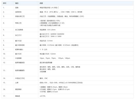
When developing a PCB manufacturing project, bridging the gap between design and production is critical to achieving efficiency and reliability. Design for Manufacturability (DFM) principles ensure your PCB layouts are optimized for real-world production, minimizing errors and reducing pcb manufacturing cost. By collaborating with experienced pcb manufacturing companies like Invotec Europe, you gain access to expert feedback early in the design phase, identifying potential bottlenecks such as impractical trace spacing, material incompatibilities, or thermal management challenges.
A key advantage of integrating DFM practices lies in avoiding costly redesigns. For instance, selecting advanced substrates or layer stack-ups that align with your application’s performance requirements can prevent delays. Below is a table highlighting common material choices and their applications:
| Material | Key Properties | Typical Applications |
|---|---|---|
| FR-4 | Cost-effective, moderate thermal | Consumer electronics, IoT |
| High-Frequency Laminates | Low signal loss, stable Dk/Df | RF, telecom, aerospace |
| Flexible Polyimide | Bendable, lightweight | Wearables, medical devices |
Adopting a proactive approach to DFM also ensures compatibility with automated assembly processes, which is vital for scaling from prototyping to high-volume production. PCB manufacturing business models that prioritize DFM—such as Invotec Europe’s—leverage simulation tools to validate designs under real-world conditions, ensuring thermal stability and signal integrity.
Moreover, tailoring designs to match industry-specific standards (e.g., automotive-grade reliability or medical device biocompatibility) reduces risks in regulated environments. By addressing pcb manufacturing challenges upfront—such as impedance control in multilayer boards or solder mask adhesion—you streamline timelines and enhance product longevity.
In essence, DFM transforms theoretical designs into manufacturable solutions, balancing innovation with practicality. Partnering with a pcb manufacturing expert ensures your project aligns with both technical requirements and budgetary constraints, turning concepts into reliable, market-ready products.
Advanced Materials and Technologies Driving High-Performance PCB Solutions
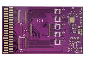
To meet the evolving demands of modern electronics, pcb manufacturing relies on cutting-edge materials and innovative technologies. High-performance solutions begin with advanced substrates like high-frequency laminates, low-loss dielectrics, and thermal management materials, which ensure signal integrity and durability in harsh environments. These materials are paired with precision fabrication techniques, such as laser direct imaging (LDI) and automated optical inspection (AOI), to achieve micron-level accuracy in trace widths and layer alignment. For pcb manufacturing companies, balancing pcb manufacturing cost with quality is critical, especially when producing complex designs like multilayer or flexible PCBs. By leveraging embedded component technology and HDI (high-density interconnect) processes, manufacturers minimize material waste and reduce assembly steps, directly addressing cost-efficiency challenges in the pcb manufacturing business.
Emerging technologies like 3D printing for rapid prototyping and AI-driven design validation further streamline production cycles, enabling faster time-to-market. Thermal simulation tools and signal integrity analysis ensure designs are optimized for performance before they reach the manufacturing floor. This proactive approach reduces rework and enhances reliability, aligning with industries such as automotive, aerospace, and medical devices, where failure is not an option. By adopting advanced plating techniques like ENEPIG (Electroless Nickel Electroless Palladium Immersion Gold), pcb manufacturing specialists achieve superior corrosion resistance and solderability, even for high-density boards.
For businesses navigating the complexities of pcb manufacturing cost, collaboration with experts who understand material trade-offs and process scalability is essential. Tailored solutions—such as hybrid rigid-flex designs or ultra-thin core substrates—empower you to meet specific application needs without over-engineering. Whether you require prototypes or large-scale production, integrating these technologies ensures your pcb manufacturing business stays ahead in a competitive, innovation-driven market.

Zero-Defect Philosophy: Ensuring Reliability in Every Circuit Board Produced
When it comes to PCB manufacturing, reliability isn’t just a goal—it’s a non-negotiable standard. Leading PCB manufacturing companies understand that even minor defects can compromise performance, safety, and longevity, especially in industries like automotive, aerospace, or medical devices. This is why a zero-defect philosophy is embedded at every stage of production, from material selection to final inspection. By leveraging advanced technologies such as automated optical inspection (AOI), X-ray testing, and rigorous electrical testing, manufacturers ensure that every layer, trace, and connection meets exact specifications.
For businesses balancing PCB manufacturing cost with quality demands, this approach minimizes risks of costly rework or field failures. Advanced process controls and real-time monitoring systems detect anomalies early, reducing waste and ensuring consistency across batches. In high-volume PCB manufacturing business environments, such precision is critical to maintaining competitiveness while adhering to strict industry certifications like ISO 9001 and IPC Class 3 standards.
Tailoring solutions to specific applications further strengthens reliability. Whether you’re integrating complex multilayer designs or working with high-frequency materials, the focus remains on eliminating variability. By collaborating closely with clients during design reviews, manufacturers identify potential pitfalls—like thermal management challenges or signal integrity issues—before they escalate. This proactive alignment between design and production not only enhances performance but also optimizes PCB manufacturing cost over the product lifecycle.
Ultimately, the zero-defect philosophy isn’t just about avoiding errors—it’s about building trust. When you partner with experts who prioritize precision at every step, you gain confidence that your circuits will perform flawlessly, even under the most demanding conditions.
Tailored Manufacturing Expertise for Industry-Specific Requirements
When it comes to PCB manufacturing, one size does not fit all. Industries such as aerospace, medical devices, automotive systems, and industrial automation each have unique demands for performance, durability, and compliance. This is where partnering with experienced PCB manufacturing companies like Invotec Europe becomes critical. Their tailored approach ensures that your industry-specific challenges—whether high-temperature resilience, signal integrity in multilayer designs, or compliance with stringent regulatory standards—are addressed through customized solutions.
By leveraging advanced fabrication techniques and material innovations, they optimize PCB manufacturing cost without compromising precision. For instance, selecting the right substrate materials or embedding specialized thermal management features can reduce long-term operational expenses while meeting exact technical specifications. This balance of cost-efficiency and quality is particularly valuable for businesses scaling their PCB manufacturing business, where minimizing waste and maximizing yield are priorities.
Invotec Europe’s expertise extends to adapting production workflows to align with your sector’s requirements. Whether you need rigid-flex PCBs for compact medical devices or high-frequency boards for telecom infrastructure, their team collaborates closely with you to refine designs for manufacturability. This proactive approach not only accelerates time-to-market but also mitigates risks associated with supply chain bottlenecks or component compatibility issues.
Moreover, their zero-defect philosophy ensures that every board—whether a prototype or a high-volume order—meets rigorous reliability standards. For industries where failure is not an option, this commitment to precision transforms PCB manufacturing from a commodity service into a strategic partnership. By integrating feedback loops and real-time testing protocols, they deliver solutions that evolve alongside your technological needs.
In essence, tailoring expertise to your industry isn’t just about solving today’s challenges—it’s about anticipating tomorrow’s innovations. With a focus on agility and technical mastery, Invotec Europe empowers your business to navigate complex PCB manufacturing landscapes confidently.
End-to-End Support: Navigating Prototyping to Large-Scale Production
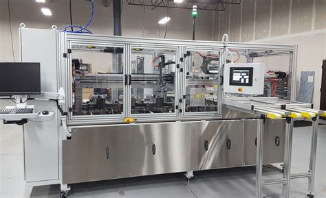
When optimizing PCB manufacturing workflows, seamless transition from prototyping to full-scale production is critical. Leading PCB manufacturing companies like Invotec Europe bridge this gap by offering comprehensive support across every stage, ensuring your designs evolve efficiently into reliable, market-ready products. Starting with prototyping, their expertise in advanced material selection and precision engineering minimizes design flaws early, reducing PCB manufacturing cost and accelerating time-to-market. By integrating design-for-manufacturability (DFM) principles, they address potential bottlenecks before production begins, ensuring scalability without compromising quality.
For businesses managing a PCB manufacturing business, balancing high-volume demands with stringent quality standards can be challenging. Invotec Europe tackles this through tailored workflows that adapt to your project’s complexity, whether you require multilayer boards for industrial automation or high-frequency PCBs for telecommunications. Their zero-defect philosophy leverages automated optical inspection (AOI) and rigorous testing protocols, guaranteeing consistency across prototypes and large batches alike. This approach not only mitigates risks but also aligns with cost-efficiency goals, as early error detection prevents costly rework.
Collaborating with a trusted partner streamlines compatibility challenges, particularly in multilayer PCB integration. Invotec Europe’s engineers provide real-time feedback during design reviews, ensuring layer alignment, thermal management, and signal integrity meet industry-specific requirements. Their end-to-end solutions also include logistics support, from material sourcing to global delivery, simplifying supply chain complexities. By unifying prototyping agility with large-scale precision, they empower you to focus on innovation while they handle the intricacies of PCB manufacturing. Whether scaling a startup or optimizing an established operation, their expertise ensures your boards perform flawlessly, every time.

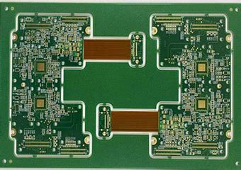
Overcoming Compatibility Challenges in Multilayer PCB Integration
Integrating multiple layers into PCB manufacturing requires balancing performance, reliability, and cost—especially as designs grow more complex. Compatibility challenges often arise from mismatched thermal expansion rates, signal interference between layers, or material inconsistencies. To address these, leading PCB manufacturing companies prioritize advanced simulation tools to model layer interactions, ensuring optimal signal integrity and thermal management. For instance, selecting materials with compatible dielectric constants and glass transition temperatures (Tg) minimizes warping and maintains stability across diverse operating conditions.
A critical factor in managing PCB manufacturing cost is streamlining layer alignment and via placement during design. Precision laser drilling and automated optical inspection (AOI) systems help maintain tight tolerances, reducing the risk of defects that could escalate expenses. Additionally, collaboration between design and production teams ensures that multilayer stacks are optimized for manufacturability, avoiding costly redesigns.
For industries like automotive or aerospace, where reliability is non-negotiable, partnering with a PCB manufacturing business that specializes in multilayer integration is essential. These providers leverage technologies such as sequential lamination and embedded component placement to enhance compatibility while meeting stringent industry standards. By adopting a proactive approach to material selection, testing, and process control, manufacturers mitigate risks and deliver boards that perform consistently under stress.
For tailored solutions, consider exploring resources like Andwin PCBA, which offers expertise in addressing multilayer challenges while aligning with your project’s technical and budgetary requirements.
Partnering with Invotec Europe: Your Trusted PCB Innovation Resource
When seeking a partner for PCB manufacturing, you need a collaborator that aligns technical expertise with your unique project goals. Invotec Europe stands out among leading PCB manufacturing companies by offering end-to-end innovation support, from conceptual design to full-scale production. Their approach begins with design-for-manufacturability (DFM) analysis, ensuring your board’s architecture is optimized for performance, scalability, and PCB manufacturing cost efficiency. By integrating advanced technologies like laser drilling and automated optical inspection (AOI), they deliver precision-engineered solutions that meet stringent quality standards, whether you’re prototyping a high-density interconnect (HDI) design or scaling up for volume production.
What sets Invotec apart in the PCB manufacturing business is their ability to tailor solutions to industry-specific challenges. For automotive, aerospace, or medical applications, their team leverages specialized materials—such as high-frequency laminates or thermal-resistant substrates—to address performance demands while maintaining cost-effectiveness. Their zero-defect philosophy ensures reliability across every production batch, minimizing risks of field failures. Additionally, their expertise in multilayer PCB integration resolves compatibility challenges, such as impedance control and signal integrity, which are critical for advanced electronics.
By collaborating with Invotec Europe, you gain access to a partner committed to transparency and agility. Their engineers provide real-time feedback during prototyping, helping you refine designs before committing to large-scale orders. This proactive approach not only accelerates time-to-market but also optimizes PCB manufacturing cost structures, ensuring your project remains economically viable without compromising quality. Whether you’re navigating complex regulatory requirements or balancing performance with budget constraints, Invotec’s tailored support transforms challenges into opportunities, solidifying their role as a trusted innovation resource in the PCB manufacturing landscape.
Conclusion
When seeking PCB manufacturing solutions that align with Europe’s stringent technical standards, partnering with established PCB manufacturing companies like Invotec Europe ensures access to expertise that balances innovation with practicality. Their focus on minimizing PCB manufacturing cost without compromising quality enables businesses to optimize budgets while leveraging advanced technologies such as high-density interconnect (HDI) boards and multilayer integration. By prioritizing design-for-manufacturability principles, Invotec streamlines the transition from prototyping to full-scale production, addressing challenges like material compatibility and thermal management. For industries with specialized needs—from aerospace to medical devices—their tailored manufacturing expertise ensures compliance with industry-specific regulations and performance benchmarks. Whether navigating the complexities of the PCB manufacturing business or scaling production efficiently, Invotec’s zero-defect philosophy and end-to-end support provide a reliable foundation for delivering durable, high-performance circuit boards. This approach not only mitigates risks but also positions your projects for long-term success in competitive markets.
Frequently Asked Questions
What defines a reliable PCB manufacturing partner for advanced technology projects?
A reliable partner combines expertise in PCB manufacturing business practices, access to cutting-edge technologies, and a zero-defect approach to quality control. Look for companies with proven experience in handling complex designs, material selection, and industry-specific compliance.
How do PCB manufacturing companies balance cost and quality?
Leading providers optimize PCB manufacturing cost through scalable production processes, material efficiency, and collaborative design reviews. By prioritizing design for manufacturability (DFM), they minimize waste while ensuring performance standards align with your project’s requirements.
What factors influence PCB manufacturing cost for multilayer designs?
Cost depends on layer count, material complexity (e.g., high-frequency substrates), precision requirements, and volume. Partnering with a manufacturer offering end-to-end prototyping reduces long-term expenses by identifying potential issues early in the development cycle.
How can businesses ensure compatibility in multilayer PCB manufacturing?
Advanced simulation tools and rigorous testing protocols are critical. Manufacturers specializing in high-density interconnect (HDI) technologies ensure seamless integration of layers, signal integrity, and thermal management, even in mission-critical applications.
Why choose Invotec Europe for PCB manufacturing business solutions?
Invotec Europe delivers tailored expertise across industries like automotive, aerospace, and telecommunications. Their zero-defect philosophy, combined with flexible prototyping and large-scale production capabilities, ensures reliable, high-performance solutions aligned with Europe’s stringent technical standards.
Ready to Streamline Your PCB Manufacturing Process?
For optimized PCB manufacturing solutions that align with your project’s unique demands, please click here to connect with experts dedicated to advancing your innovation.