How to achieve exponential growth in PCB design efficiency of LED screens?
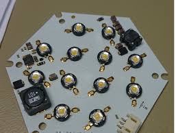
LED has appeared in all aspects of life, such as radio and television, media, exhibitions, remote video interaction, office, conference, etc. Larger, thinner, clearer, high-density and small-pitch LED screens have become a major development trend, which means that higher requirements are placed on the PCB design of LED screens. Because a high-quality PCB design is an important foundation for the integration and integration of LED screens, and it has also become one of the foundations for enterprises to reflect product differentiation.
If you want to do your work well, you must first sharpen your tools.
A good PCB design software must have efficient system operation and good operation fluency. However, with the increasing complexity of PCB design, many companies are facing the situation of lagging design software operation and greatly reduced system fluency. At the same time, how to use design software to quickly bring mature PCB design solutions in LED screens into the design of new products to improve quality and efficiency, and to open up the cooperation between PCB design engineers and structural departments to achieve better design innovation has also become a pain point faced by many companies. Various challenges have become problems that customers need to solve urgently in a highly competitive and rapidly developing market environment.
In response to these challenges, Siemens EDA’s PADS Professional helps developing companies keep up with the market and solve difficulties, while improving the work efficiency of LED screen PCB design engineers, optimizing design quality and promoting product innovation.
Software operation ability is improved, and design work efficiency is doubled
Siemens EDA has been deeply involved in the market for many years. For existing PADS users, its simplicity, ease of use, flexibility, and fast data control meet the most basic panel design needs of PCB design engineers. Compared with 32-bit PADS, PADS Professional is directly expanded to 64 bits while ensuring easy learning and use, and adding more modules and functions. Its functions are powerful enough to meet the most complex and demanding design requirements, and solve the problems of existing customers in the process of using PADS. When designing more and more complex PCB panels, the operation speed lags and the jamming process occur.
For the daily basic operations of PCB design engineers such as layout, wiring, etc., the operation ability of PADS Professional drawing board design tools is faster and stronger than PADS, which can improve the work efficiency of PCB designers by a full 3 times. As the software running speed is greatly improved, its operation fluency and compatibility have greater room for display, directly helping customers shorten the product design cycle and accelerate the product to market.
“Modular” reuse PCB designers get rid of “starting from scratch”
In the PCB design of LED screens, although different products have different structures, their connection relationships are essentially the same. Generally speaking, 60%-70% of the PCB design of a new product will follow the previously mature design scheme, and the traditional practice of designers is to copy and paste the required structure to the new design drawing, which is cumbersome and complicated, and is not conducive to improving work efficiency. The modular reuse function of PADS Professional can solve this pain point, that is, the software automatically imports the part that can be directly applied in the mature solution to the maximum extent and in the most convenient and quick way into the new design.
Specifically, PADS Professional not only imports the connection relationship of the circuit diagram in the original design, but its modular reuse function can copy the corresponding relationship of the schematic diagram in the mature solution, including the network connection of the signal, the connection relationship at the physical level of the PCB Layout, etc. In addition, in the process of designing new products and using modular reuse, designers do not need to worry about the compatibility of new and old designs. For example, if different parts are needed in the new PCB design, the design engineer will automatically receive a prompt interface to present the historical data and existing parameters of the reused parts during the use of the software, and show the differences in details between the two through the comparison of the schematic diagram, so that engineers can quickly and accurately select the lines and layouts that need to be reused. This function helps PCB design engineers avoid a series of repetitive, time-consuming and laborious mechanical operations, and helps to devote their energy to designs that need to be modified, improved and innovated, allowing engineers to get rid of “starting from scratch”, greatly speeding up the progress and work efficiency of the design project.
Electronics (ECAD) and mechanics (MCAD) run together, and the integrated environment achieves seamless connection
As LED screens are getting thinner and thinner, there are more requirements for the design of their structural parts. In the traditional process, the design drawings of structural engineers must be output in the form of documents and handed over to electronic engineering designers. Designers then import and open the documents, and according to the requirements of the structural design department, they can start PCB design after finding a series of key information. The whole process is cumbersome and requires high communication costs. PADS Professional directly integrates ECAD and MCAD in an integrated environment, allowing barrier-free communication and cooperation between the electronic design department and the structural design department, avoiding costly design rework.
For example, when the structural engineer has designed the design frame, housing, USB interface, video interface position, etc
., he can directly import the designed drawing board and the required information into the PADS Professional platform through electronic data transmission. The electronic design engineer can directly use the key information such as the position and coordinates of the machine key, eliminating the process of manual search and input, and also avoiding the errors caused by manual input errors when matching with the structural department. Since structural design is fixed in many aspects, PCB electronic engineers can sort out multiple high-quality design alternatives under the fixed basic framework, and these solutions can also interact with structural engineers at any time with one click and get timely feedback.
As a bridge connecting the two key design fields of ECAD and MCAD, PCB encourages collaborative work as soon as a problem is found or a more optimized solution is available, and never delays solving the corresponding problems until the design handover. In other words, since structural engineers and electronic engineers can use PADS Professional at any time to conduct multiple interactive internal cycles, the one-click transmission of electronic data eliminates the need for information that could only be transmitted through traditional communication methods such as telephone and email, which is enough to help the entire design plan achieve a leap in quality in a shorter time.