Streamlining Circuit Board Assembly: Key Strategies for Success
Key Takeaways
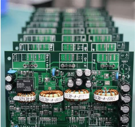
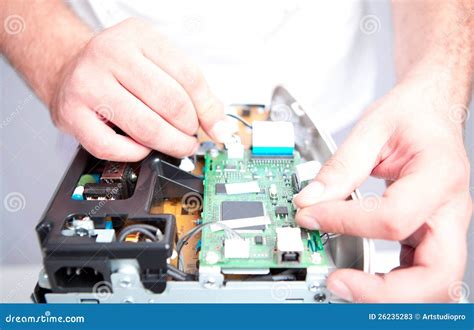
Successful PCB assembly hinges on balancing efficiency, precision, and cost-effectiveness. A core strategy involves design optimization, where layouts are simplified to minimize errors during component placement and soldering. This reduces rework and accelerates production timelines. Integrating automation in PCBA workflows—such as pick-and-place systems and robotic soldering—ensures consistency while scaling output.
Advanced quality testing methods, like automated optical inspection (AOI) and X-ray analysis, play a pivotal role in detecting flaws early, preventing costly post-production fixes. Adopting cost-effective production tools, such as modular jigs or standardized component libraries, further streamlines operations.
Tip: Prioritize cross-functional collaboration between design and manufacturing teams to identify potential bottlenecks before assembly begins.
Effective component management—including lifecycle tracking and supplier diversification—mitigates delays caused by shortages or obsolescence. Additionally, embracing Industry 4.0 technologies, such as IoT-enabled monitoring and predictive maintenance, enhances real-time decision-making. Finally, continuous workforce training ensures teams stay adept with evolving tools and techniques, fostering a culture of innovation and adaptability in PCB assembly processes.
Design Optimization for Enhanced Assembly Efficiency
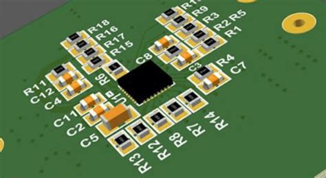
Design optimization is a foundational step in improving PCB assembly efficiency, as it directly impacts manufacturability, cost, and reliability. By prioritizing design for manufacturability (DFM) principles, engineers can minimize errors, reduce rework, and accelerate production timelines. Key strategies include simplifying component placement to avoid overcrowding, which reduces the risk of solder bridging and misalignment during PCBA. Utilizing standardized footprint libraries ensures compatibility with automated pick-and-place systems, while optimizing trace routing minimizes signal interference and thermal hotspots.
Incorporating panelization techniques—grouping multiple boards into a single panel—streamlines handling during assembly and testing, especially for high-volume production. Additionally, designing for automated inspection (e.g., including fiducial markers and test points) enhances accuracy in PCB assembly workflows. Thermal management is another critical consideration; integrating heat dissipation features like thermal vias or heatsink placements during the design phase prevents performance degradation in finished PCBA units.
Software tools such as electronic design automation (EDA) platforms enable real-time collaboration between design and manufacturing teams, identifying potential issues like insufficient clearances or incompatible materials early in the process. By balancing performance requirements with practical assembly constraints, organizations can achieve a seamless transition from prototype to mass production. This proactive approach not only cuts costs but also ensures that PCB assembly processes align with evolving industry standards, laying the groundwork for scalable and repeatable manufacturing success.
Integrating Automation in Circuit Board Manufacturing
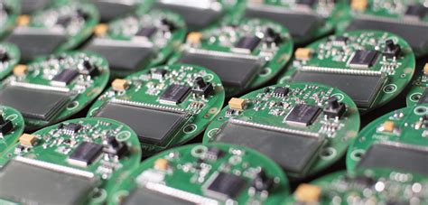
The adoption of automation in PCB assembly has revolutionized manufacturing workflows, enabling faster production cycles and higher consistency. By integrating robotic systems, such as pick-and-place machines and automated soldering stations, manufacturers can reduce human error while scaling output. For instance, PCBA lines equipped with vision-guided robotics ensure precise component placement, even for micro-scale parts, which is critical for high-density boards.
A key advantage of automation lies in its ability to streamline repetitive tasks. Automated optical inspection (AOI) systems, for example, scan boards for defects like misaligned components or soldering flaws, ensuring compliance with strict quality standards. This reduces rework rates and accelerates time-to-market. Additionally, machine learning algorithms can analyze production data to predict maintenance needs, minimizing downtime.
| Automation Tool | Function | Impact on PCBA |
|---|---|---|
| Robotic Pick-and-Place | Component placement | 95%+ placement accuracy |
| AOI Systems | Defect detection | 30% faster inspection cycles |
| Automated Soldering | Solder application | Consistent joint quality |
| Conveyor Systems | Material handling | 50% reduction in manual handling |
To maximize efficiency, manufacturers should prioritize modular automation solutions that adapt to evolving PCB assembly requirements. For example, flexible manufacturing cells can be reconfigured for different product batches, supporting small-to-medium runs without sacrificing speed. This approach is particularly valuable in industries like aerospace or medical devices, where customization is common.
However, successful integration requires balancing upfront investments with long-term gains. While automated systems lower labor costs and enhance precision, they demand rigorous calibration and skilled oversight. Training programs focused on PCBA-specific automation software and hardware ensure operators can troubleshoot issues and optimize workflows.
By aligning automation with Industry 4.0 principles—such as IoT-enabled monitoring and real-time data exchange—manufacturers can create a cohesive ecosystem. This not only boosts PCB assembly efficiency but also positions facilities for future advancements in smart manufacturing.
Advanced Quality Testing Methods for Precision
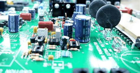
Achieving precision in PCB assembly demands rigorous quality testing methods that identify defects early while maintaining production efficiency. Modern PCBA workflows leverage automated optical inspection (AOI) systems, which use high-resolution cameras and machine learning algorithms to scan boards for soldering defects, component misalignment, or missing parts. These systems compare captured images against design specifications, flagging discrepancies with micron-level accuracy. For hidden connections, such as those in ball grid array (BGA) components, X-ray inspection provides non-destructive analysis, revealing voids, cracks, or insufficient solder under the surface.
In-circuit testing (ICT) remains a cornerstone for functional validation, applying electrical signals to verify component performance and circuit integrity. Advanced ICT setups integrate boundary-scan techniques to test complex digital circuits, reducing dependency on physical probes. Environmental stress testing, including thermal cycling and humidity exposure, simulates real-world conditions to ensure reliability over a product’s lifecycle.
To minimize human error, manufacturers increasingly adopt automated test equipment (ATE), which streamlines repetitive checks and generates detailed reports for traceability. Pairing these tools with statistical process control (SPC) software enables real-time monitoring of production trends, allowing teams to address deviations before they escalate. For high-mix, low-volume PCBA scenarios, flying probe testers offer flexibility by adapting to diverse board layouts without custom fixtures.
Emerging technologies like 3D solder paste inspection (SPI) further enhance precision by measuring paste volume and alignment before reflow, preventing defects at the source. Combined with closed-loop feedback systems, these methods create a proactive quality framework, reducing rework costs and accelerating time-to-market. By integrating data-driven testing protocols with Industry 4.0 principles, manufacturers ensure that every PCB assembly meets stringent standards while adapting to evolving technological demands.
Cost-Effective Production Techniques and Tools
Achieving cost-effective production in PCB assembly demands a balance between resource optimization and maintaining high-quality standards. One foundational strategy is leveraging design for manufacturability (DFM) principles early in the PCBA process. By simplifying layouts, standardizing component sizes, and minimizing complex routing, manufacturers reduce material waste and assembly time. For instance, using standardized footprints for components like resistors or capacitors ensures compatibility with automated placement systems, lowering rework rates. Additionally, modular design approaches allow for reusable subassemblies, cutting development costs for future projects.
Integrating automation tools such as pick-and-place machines and automated optical inspection (AOI) systems streamlines workflows while reducing labor expenses. These technologies not only accelerate throughput but also enhance precision, minimizing errors that lead to costly revisions. For small to medium batches, flexible manufacturing systems (FMS) enable rapid reconfiguration of assembly lines, optimizing resource utilization without sacrificing scalability.
Adopting lean manufacturing principles further drives down costs. Techniques like Just-in-Time (JIT) inventory management reduce excess stockpiling of components, while predictive maintenance schedules for equipment prevent unplanned downtime. Pairing these practices with energy-efficient soldering systems and smart power management solutions lowers operational overhead, contributing to long-term savings.
Investing in scalable tooling solutions, such as modular jigs or programmable soldering stations, allows manufacturers to adapt to varying production volumes without significant capital expenditure. Similarly, utilizing cloud-based production monitoring software provides real-time insights into inefficiencies, enabling data-driven adjustments. For example, identifying bottlenecks in solder paste application can lead to targeted process refinements, reducing material waste.
Finally, fostering strategic supplier partnerships ensures access to high-quality components at competitive prices. Bulk purchasing agreements and collaborative forecasting with suppliers mitigate supply chain disruptions, while local sourcing of critical parts reduces lead times. By combining these techniques, businesses can achieve cost-effective PCB assembly without compromising on reliability or performance, positioning themselves competitively in fast-paced electronics markets.
Streamlining Workflow Processes for Faster Turnaround
Efficient PCB assembly relies heavily on optimizing workflow processes to minimize delays and maximize throughput. A streamlined workflow begins with evaluating each stage of the PCBA production cycle, from component procurement to final testing. By mapping out interdependencies and identifying bottlenecks, manufacturers can implement lean manufacturing principles to eliminate redundant steps and reduce idle time. For instance, integrating automated inventory management systems ensures real-time tracking of components, preventing shortages that might stall production.
Adopting standardized protocols for design file handoffs between engineering and manufacturing teams is another critical step. Clear communication reduces errors and rework, which are common time sinks in PCB assembly. Additionally, modular workstation layouts and cross-trained personnel enable flexible resource allocation, allowing teams to adapt swiftly to shifting priorities. Tools like digital twin simulations can further refine workflows by modeling production scenarios and predicting potential inefficiencies before physical assembly begins.
Automation plays a pivotal role in accelerating PCBA workflows. Robotic systems for tasks like solder paste application, component placement, and optical inspection not only speed up processes but also enhance consistency. Pairing these systems with AI-driven analytics helps identify patterns in production delays, enabling proactive adjustments. For example, predictive maintenance algorithms can alert teams to equipment wear before it causes downtime.
Finally, adopting agile project management frameworks, such as Kanban or Scrum, ensures continuous progress tracking and rapid response to issues. By combining these strategies, manufacturers can achieve faster turnaround times without compromising quality, positioning themselves to meet tight deadlines and evolving market demands.
Effective Component Selection and Management Strategies
Selecting and managing components effectively is foundational to optimizing PCB assembly workflows. A well-structured approach begins with aligning component specifications with design requirements, ensuring compatibility across thermal, electrical, and mechanical parameters. Prioritizing PCBA-ready components—such as standardized surface-mount devices (SMDs) or through-hole parts—reduces redesign efforts and accelerates production timelines. Leveraging supplier partnerships for long-lead-time items or obsolete parts mitigates delays, while digital inventory systems enable real-time tracking of stock levels, minimizing overstocking or shortages.
Standardizing component libraries within design software streamlines PCB assembly by reducing errors during placement and soldering. For instance, using pre-validated footprints and symbols ensures consistency, especially in high-mix manufacturing environments. Additionally, integrating lifecycle management tools helps identify components nearing end-of-life, allowing proactive substitutions before they disrupt production. This is critical in industries like aerospace or medical devices, where reliability and compliance are non-negotiable.
Automated tools for bill of materials (BOM) validation further enhance accuracy by flagging mismatches in tolerances, ratings, or packaging early in the design phase. Pairing this with just-in-time (JIT) procurement strategies reduces storage costs and ensures fresher components, which is vital for moisture-sensitive parts like BGAs or QFNs. For cost-sensitive projects, evaluating alternative components with equivalent performance but lower costs—without compromising quality—can yield significant savings.
Finally, fostering collaboration between design and procurement teams ensures alignment on component availability and cost targets. By embedding PCBA-centric thinking into the design process, manufacturers can avoid rework, reduce cycle times, and maintain high yields. This holistic approach to component management not only enhances efficiency but also builds resilience against supply chain volatility.
Implementing Continuous Improvement and Workforce Training
Achieving long-term success in PCB assembly and PCBA manufacturing requires a dual focus on refining processes and investing in human capital. Continuous improvement methodologies, such as Lean Six Sigma, enable teams to systematically identify bottlenecks, reduce waste, and enhance workflow consistency. For instance, regular audits of surface-mount technology (SMT) placement accuracy or solder paste application can uncover opportunities for incremental enhancements. Pairing these practices with cross-functional collaboration ensures that insights from design, production, and testing teams inform iterative refinements.
Equally critical is workforce training tailored to evolving PCB assembly technologies. As automation and Industry 4.0 tools become integral to PCBA lines, technicians must stay adept at operating advanced machinery, interpreting real-time analytics, and troubleshooting complex systems. Structured programs—such as certifications in automated optical inspection (AOI) or hands-on workshops for reflow oven optimization—bridge skill gaps and empower employees to adapt to new workflows. Additionally, fostering a culture of knowledge-sharing through mentorship or digital training platforms ensures that best practices are consistently applied across shifts.
To sustain progress, organizations should implement feedback loops where frontline workers contribute ideas for process improvements. Metrics like defect rates, cycle times, and equipment uptime can guide targeted training initiatives, while data-driven dashboards provide visibility into performance trends. By aligning continuous improvement with a skilled, adaptable workforce, manufacturers can maintain high-quality PCB assembly outputs while scaling operations efficiently.
Leveraging Industry 4.0 for Future-Ready Assembly
The integration of Industry 4.0 technologies is revolutionizing PCB assembly (PCBA), enabling manufacturers to achieve unprecedented levels of precision, scalability, and adaptability. By embedding smart systems such as IoT-enabled sensors, AI-driven analytics, and automated workflows, modern PCBA processes can seamlessly synchronize design, production, and testing phases. For instance, real-time data collection from connected machinery allows for instant adjustments in assembly lines, minimizing errors and reducing downtime. This interconnected approach ensures that PCB assembly workflows are not only faster but also more responsive to dynamic market demands.
Central to this transformation is the adoption of digital twin technology, which creates virtual replicas of physical PCBA systems. These models simulate production scenarios, identify bottlenecks, and optimize resource allocation before physical implementation. Coupled with machine learning algorithms, manufacturers can predict component failures, streamline inventory management, and enhance traceability across supply chains. Automation tools like robotic pick-and-place systems further amplify efficiency, handling intricate tasks with micron-level accuracy while maintaining consistency in high-volume production.
Moreover, Industry 4.0 fosters collaboration between humans and machines. Advanced augmented reality (AR) interfaces guide technicians through complex assembly procedures, reducing training time and improving error detection. Meanwhile, cloud-based platforms centralize design files, test results, and quality metrics, ensuring stakeholders access unified data for informed decision-making. By prioritizing cybersecurity protocols and interoperable standards, these systems safeguard intellectual property and maintain compliance in globally distributed operations.
Ultimately, embracing Industry 4.0 in PCB assembly isn’t merely about adopting new tools—it’s about building a resilient ecosystem where agility and innovation drive competitiveness. Manufacturers who leverage these advancements position themselves to meet evolving customer expectations while scaling production sustainably.
Conclusion
In the rapidly evolving landscape of PCB assembly (PCBA), achieving operational excellence hinges on the strategic integration of multiple best practices. Prioritizing design optimization ensures that boards are not only functional but also tailored for manufacturability, reducing errors and rework. The adoption of automation integration—from pick-and-place systems to AI-driven inspection tools—accelerates production while maintaining consistency across high-volume orders. Equally critical are advanced quality testing methods, such as automated optical inspection (AOI) and X-ray analysis, which safeguard precision in complex, miniaturized components.
Cost efficiency remains a cornerstone of successful PCBA workflows, achievable through lean manufacturing principles and investments in scalable tools like modular assembly lines. Streamlining workflows further demands meticulous component management, including just-in-time sourcing and digital inventory tracking, to mitigate delays. Equipping teams with continuous improvement frameworks and cross-functional training fosters adaptability, ensuring that workforce expertise aligns with technological advancements.
Finally, embracing Industry 4.0 technologies—IoT-enabled monitoring, predictive maintenance, and real-time data analytics—positions manufacturers to meet future demands for smarter, interconnected PCB assembly systems. By harmonizing these strategies, businesses can achieve faster turnaround times, higher yield rates, and sustained competitiveness in an increasingly dynamic market. The path to success lies not in isolated improvements but in a holistic approach that balances innovation, quality, and agility.
Frequently Asked Questions
What are the primary challenges in modern PCB assembly workflows?
The main challenges include balancing design complexity with manufacturability, ensuring component availability, maintaining quality control, and adapting to rapid technological advancements. Design for Manufacturability (DFM) principles and advanced PCBA testing tools help address these issues.
How does automation improve PCB assembly efficiency?
Automation reduces human error, accelerates production cycles, and ensures consistency. Technologies like pick-and-place systems and automated optical inspection (AOI) streamline PCBA processes, while robotic soldering enhances precision in high-volume projects.
What role does quality testing play in PCB assembly?
Quality testing ensures reliability and functionality. Techniques such as AOI, X-ray inspection, and functional testing identify defects early, minimizing rework. Implementing these methods in PCBA workflows reduces costs and boosts customer confidence.
How can manufacturers achieve cost-effective production in PCB assembly?
Strategies include optimizing panel layouts to reduce material waste, leveraging bulk purchasing for components, and adopting modular PCBA designs. Investing in scalable tools like reflow ovens and 3D solder paste inspection also enhances long-term savings.
What steps streamline workflow in PCB assembly projects?
Standardizing processes, using digital twin simulations for design validation, and integrating real-time monitoring systems improve workflow efficiency. Adopting lean manufacturing principles in PCBA reduces bottlenecks and accelerates turnaround times.
Why is component management critical in PCB assembly?
Effective management prevents delays caused by shortages or obsolescence. Tools like component lifecycle tracking and supplier collaboration platforms ensure seamless PCBA production. Prioritizing common component libraries also simplifies design phases.
How does workforce training impact PCB assembly outcomes?
Continuous training ensures teams stay updated on Industry 4.0 tools like IoT-enabled equipment and AI-driven analytics. Skilled personnel reduce errors and adapt faster to evolving PCBA standards, driving overall productivity.
What future trends will shape PCB assembly?
Advances in smart manufacturing, such as AI-powered defect detection and collaborative robotics, will dominate. Embracing modular automation and data-driven decision-making will keep PCBA processes competitive in a dynamic market.
Ready to Optimize Your PCB Assembly Process?
Explore tailored solutions for your PCBA needs. For expert guidance on streamlining your workflow, please click here: https://www.andwinpcb.com/pcb-assembly/.