Streamlining Compact PCB Assembly and Testing for Precision Electronics
Key Takeaways
Efficient PCB assembly and testing in compact electronics demand a balance between precision, scalability, and reliability. The shift toward miniaturized components necessitates automated placement systems to achieve sub-millimeter accuracy, reducing human error in high-density PCBA workflows. Advanced techniques like laser-assisted soldering and 3D inspection tools ensure consistent quality, particularly for delicate components such as microcontrollers or ultra-thin connectors.
Integrating automated testing protocols—such as in-circuit testing (ICT) and boundary scan—streamlines validation, enabling rapid fault detection in complex circuits. For example, automated optical inspection (AOI) systems can identify soldering defects at speeds unattainable through manual methods. Below is a comparison of common testing methods:
| Testing Method | Purpose | Key Benefit |
|---|---|---|
| Automated Optical Inspection (AOI) | Detects soldering defects | High-speed visual analysis |
| X-ray Inspection | Examines hidden joints (e.g., BGA) | Non-destructive internal assessment |
| Functional Testing | Validates overall circuit behavior | Ensures end-use performance |
Workflow optimization further hinges on modular design principles, which simplify component placement and reduce cross-functional dependencies. Pairing these strategies with predictive maintenance for assembly machinery minimizes downtime, while traceability systems track components from procurement to final testing. Case studies in medical devices and IoT sensors highlight how standardized PCBA protocols reduce rework rates by up to 40%, underscoring the value of integrating error-proofing steps like sequential verification checkpoints.
Ultimately, achieving reliability in compact electronics relies on harmonizing cutting-edge PCB assembly technologies with rigorous quality frameworks, ensuring scalability without compromising precision.
Introduction to Compact PCB Assembly in Precision Electronics
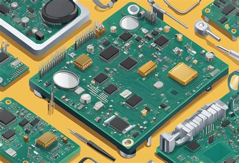
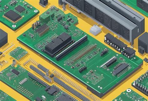
The demand for miniaturized electronics has driven significant advancements in PCB assembly techniques, particularly for applications requiring high precision and reliability. Compact PCB assembly (PCBA) involves the intricate process of placing, soldering, and testing electronic components on densely populated, small-scale circuit boards. These assemblies form the backbone of modern devices—from medical implants to aerospace systems—where space constraints and performance accuracy are non-negotiable.
A critical aspect of PCBA in precision electronics is balancing component density with thermal and electrical integrity. As components shrink, challenges such as signal interference, heat dissipation, and mechanical stability become more pronounced. Advanced surface-mount technology (SMT) and automated pick-and-place systems enable precise positioning of micro-components, reducing human error and ensuring consistent solder joint quality. For instance, using vision-guided robotics allows for real-time adjustments during placement, which is vital for maintaining alignment in high-density layouts.
Tip: Implement pre-assembly simulations to identify potential thermal hotspots or signal integrity issues early in the design phase, minimizing rework during production.
Testing is equally crucial in compact PCB assembly. Automated optical inspection (AOI) and X-ray testing are employed to detect defects like micro-cracks or bridged solder joints that are invisible to the naked eye. Pairing these with in-circuit testing (ICT) ensures functional validation, verifying that every resistor, capacitor, and IC operates within specified parameters.
Workflow optimization further enhances efficiency. Modular assembly lines, combined with just-in-time inventory management, reduce lead times and material waste. Additionally, adopting error-proofing protocols, such as barcode scanning for component verification, prevents mismatches during the PCBA process.
As industries push the boundaries of miniaturization, the role of compact PCB assembly continues to evolve, demanding tighter integration between design, assembly, and testing phases. By leveraging advanced technologies and robust quality control measures, manufacturers can achieve the precision required for next-generation electronics while maintaining scalability and cost-effectiveness.
Key Challenges in Miniaturized Electronic Component Assembly
The shift toward compact electronics has intensified the complexity of PCB assembly and testing, particularly when dealing with miniaturized components. One primary challenge lies in achieving precise placement of microscopic parts, such as 01005 resistors or ultra-fine-pitch ICs, which demand advanced PCBA equipment and meticulous calibration. Even minor misalignments during soldering can lead to defects like bridging or cold joints, compromising the functionality of high-density boards. Thermal management also becomes critical, as densely packed components generate localized heat, raising the risk of thermal stress and long-term reliability issues.
Another hurdle is maintaining signal integrity in tightly spaced layouts. Crosstalk and electromagnetic interference (EMI) are amplified in miniaturized designs, necessitating rigorous pre-assembly simulations and post-production testing. Additionally, the integration of mixed-technology components—such as combining surface-mount devices (SMDs) with through-hole parts—requires hybrid PCB assembly workflows, which can introduce bottlenecks if not optimized.
Testing and inspection further complicate the process. Traditional probe-based methods struggle to access test points on ultra-compact boards, driving the need for automated optical inspection (AOI) and X-ray imaging. However, these technologies add cost and time, especially when verifying solder joints under ball grid arrays (BGAs) or chip-scale packages (CSPs). Finally, material selection plays a pivotal role. Substrates with low thermal expansion coefficients and high-temperature resilience are essential to prevent warping during reflow soldering, yet these materials often come at a premium.
Addressing these challenges demands a balance between precision engineering, advanced PCBA tools, and adaptive quality control frameworks to ensure both efficiency and reliability in modern electronics manufacturing.
Advanced Techniques for Efficient PCB Component Placement
Achieving precision in PCB assembly for compact electronics demands a strategic approach to component placement, particularly as devices shrink and functionality expands. Central to this process is the integration of surface-mount technology (SMT), which enables the placement of smaller, high-density components like microcontrollers and 0402 passives with minimal spacing. Advanced pick-and-place systems equipped with machine vision and AI-driven algorithms optimize accuracy, reducing misalignment risks even in high-density PCB designs. These systems prioritize component sequencing to minimize toolhead travel time, enhancing throughput without compromising placement precision.
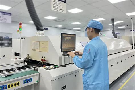
Another critical technique involves thermal management during assembly. Components in tightly packed layouts generate heat that can affect solder joint integrity. Pre-assembly simulations using thermal imaging tools help identify hotspots, guiding designers to adjust component positioning or incorporate thermally conductive substrates. Additionally, automated solder paste inspection (SPI) ensures uniform deposition, mitigating defects before reflow. For PCBA workflows, combining in-circuit testing (ICT) with automated optical inspection (AOI) at intermediate stages allows real-time validation of component functionality and orientation, reducing rework cycles.
Workflow optimization further hinges on modular assembly strategies, where multi-stage processes are segmented to address specific challenges. For example, placing sensitive analog components first minimizes exposure to heat from subsequent soldering stages. Collaborative robotics (cobots) assist in handling delicate parts, ensuring repeatability in miniaturized PCB assembly. Finally, data-driven analytics track placement accuracy and defect rates, enabling iterative refinements to both design and assembly protocols. By harmonizing these techniques, manufacturers can achieve error-minimized PCBA workflows, ensuring reliability in precision-critical applications.
Implementing Automated Testing for Enhanced Reliability
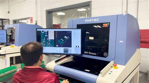
Automated testing has become a cornerstone of modern PCB assembly processes, particularly in high-density applications where precision and reliability are non-negotiable. By integrating advanced inspection systems such as automated optical inspection (AOI) and X-ray inspection (AXI), manufacturers can identify defects like solder bridging, misaligned components, or voids in real time. These systems complement PCBA workflows by scanning boards at micron-level resolutions, ensuring even the smallest discrepancies in compact layouts are flagged before final integration. For example, AOI leverages machine vision algorithms to compare assembled boards against digital templates, while AXI penetrates layered structures to inspect hidden connections—critical for multilayer or buried-component designs.
To further minimize human error, in-circuit testing (ICT) and functional testing are automated to validate electrical performance post-assembly. ICT checks continuity, resistance, and capacitance across circuits, while functional testing simulates real-world operating conditions to verify board behavior. By embedding these protocols directly into the PCBA production line, teams reduce manual intervention, accelerate throughput, and maintain consistency across batches. Additionally, adaptive test scripting allows systems to dynamically adjust parameters based on component tolerances or design revisions, ensuring flexibility in high-mix manufacturing environments.
Data analytics also play a pivotal role in enhancing reliability. Automated testing generates vast datasets, which machine learning models analyze to predict failure trends or optimize test coverage. For instance, identifying recurring faults in specific PCB assembly stages enables preemptive adjustments to soldering profiles or pick-and-place algorithms. This proactive approach not only elevates yield rates but also aligns with stringent quality standards like IPC-A-610, which governs acceptability criteria for electronic assemblies.
Ultimately, the synergy between automated inspection, electrical validation, and data-driven insights creates a robust framework for error-free PCBA production. By prioritizing these methodologies, manufacturers ensure that compact electronics meet the exacting demands of industries such as medical devices, aerospace, and IoT—where reliability is synonymous with safety and performance.

Workflow Optimization Strategies for Error Reduction
Efficient PCB assembly in compact electronics demands systematic workflow optimization to minimize errors while maintaining precision. A critical first step involves integrating design-for-manufacturability (DFM) principles early in the development cycle, ensuring component layouts align with PCBA capabilities. By simulating assembly processes using advanced software, engineers can identify potential bottlenecks, such as inadequate solder paste deposition or component placement conflicts, before physical prototyping. Automated optical inspection (AOI) systems further reduce human error by validating solder joint quality and component alignment in real time, particularly crucial for high-density boards where even micron-level deviations impact performance.
Standardizing assembly protocols, such as using pick-and-place machines with vision-guided accuracy, ensures consistent PCB assembly across batches. Pairing this with traceability systems—such as barcodes or RFID tags—enables rapid root-cause analysis if defects arise. For testing phases, combining in-circuit testing (ICT) with boundary-scan techniques streamlines fault detection in densely packed circuits, while machine learning algorithms analyze historical data to predict and preempt recurring issues. Modular workflows, where assembly and testing stages are segmented into discrete, repeatable steps, also enhance scalability and simplify troubleshooting.
To address thermal and mechanical stresses inherent in miniaturized PCBA, controlled environmental conditions—such as humidity-regulated workspaces and precision reflow ovens—maintain process stability. Cross-functional collaboration between design, manufacturing, and quality assurance teams further tightens feedback loops, ensuring iterative improvements. By embedding error-proofing mechanisms like poka-yoke (mistake-proofing) fixtures and statistical process control (SPC) charts, manufacturers achieve higher first-pass yields, reducing rework costs and accelerating time-to-market for precision electronics.
Quality Control Protocols in High-Density PCB Assembly
In high-density PCB assembly, rigorous quality control protocols are essential to ensure the reliability of precision electronics. As components shrink and interconnect densities rise, traditional inspection methods often fall short in detecting microscopic defects. Modern PCBA workflows integrate automated optical inspection (AOI) and X-ray imaging to identify issues like solder bridging, component misalignment, or voids in ball grid arrays (BGAs). These tools enable non-destructive testing while maintaining throughput, critical for compact designs where even minor flaws can compromise functionality.
To address variability in high-density PCB assembly, manufacturers employ statistical process control (SPC), which monitors production metrics in real time. By analyzing trends in solder paste deposition, placement accuracy, and reflow profiles, teams can make proactive adjustments to minimize deviations. Additionally, in-circuit testing (ICT) and functional testing validate electrical performance post-assembly, ensuring that embedded microcontrollers, sensors, and power management ICs operate within specified parameters.
Environmental stress testing further reinforces reliability, exposing assembled boards to thermal cycling, vibration, and humidity to simulate real-world conditions. For PCBA in mission-critical applications, traceability systems document every component’s origin, placement data, and test results, streamlining root-cause analysis if failures occur. By combining these protocols with closed-loop feedback systems, manufacturers achieve near-zero defect rates, aligning with stringent industry standards while supporting scalable production of miniaturized electronics.
Case Studies: Successful Applications of Streamlined Processes
Recent advancements in PCB assembly and PCBA workflows have demonstrated measurable improvements in precision electronics manufacturing. For instance, a medical device manufacturer adopted automated pick-and-place systems integrated with machine vision to handle miniature components on high-density boards. This approach reduced placement errors by 40% while accelerating production cycles, proving critical for implantable devices requiring flawless PCB assembly. Another case involved a consumer electronics firm specializing in wearable technology. By implementing real-time automated testing protocols during PCBA, the company identified solder joint defects early, cutting post-production rework costs by 30% and ensuring compliance with stringent reliability standards.
In the automotive sector, a supplier of advanced driver-assistance systems (ADAS) leveraged modular testing frameworks to validate compact PCB assemblies under extreme environmental conditions. By combining thermal cycling tests with automated optical inspection (AOI), the team achieved a 98% first-pass yield rate, minimizing delays in high-volume production. Similarly, an aerospace contractor optimized their PCBA workflow using predictive analytics to preempt component mismatches in densely packed avionics boards, reducing assembly-related downtime by 25%.
These examples underscore how strategic integration of PCB assembly automation and PCBA testing innovations can address scalability and precision demands. The medical and automotive cases, in particular, highlight the importance of error-minimizing protocols in industries where component failure carries significant risks. By prioritizing workflow optimization, manufacturers not only enhance efficiency but also future-proof their processes against evolving miniaturization challenges.
Future Trends in Compact PCB Assembly and Testing Technology
The evolution of PCB assembly and PCBA technologies is poised to address the growing demand for miniaturized, high-performance electronics. Emerging trends emphasize integrating AI-driven analytics and machine learning into compact PCB workflows, enabling real-time defect detection and predictive maintenance during assembly. Innovations like 3D-printed circuit structures and embedded component packaging are redefining design flexibility, allowing for ultra-dense layouts without compromising reliability. Advanced PCBA processes now leverage robotic precision for placing micro-components, reducing human error while accelerating throughput.
Another critical shift involves the adoption of modular testing frameworks that combine automated optical inspection (AOI) with in-circuit testing (ICT), ensuring comprehensive validation of high-density PCBs. These systems utilize adaptive algorithms to identify marginal failures in soldering or component alignment, even in sub-millimeter geometries. Additionally, the rise of flexible hybrid electronics (FHE) is pushing boundaries in wearable and IoT devices, demanding novel assembly techniques for stretchable substrates and conformal coatings.
Sustainability is also shaping future PCB assembly practices, with a focus on eco-friendly materials and energy-efficient manufacturing. Innovations like laser-assisted depaneling and low-temperature soldering minimize thermal stress on delicate components, enhancing longevity. Meanwhile, digital twin simulations are becoming integral to PCBA workflows, enabling virtual prototyping to preempt design flaws before physical production.
As the industry moves toward smart factories, interconnected IoT systems will synchronize assembly, testing, and quality control into seamless, data-driven pipelines. This integration not only optimizes resource allocation but also ensures traceability across the supply chain, critical for sectors like medical devices and aerospace. The convergence of these technologies promises to elevate precision, scalability, and sustainability in compact PCB manufacturing, setting new benchmarks for next-generation electronics.
Conclusion
The evolution of PCB assembly and testing methodologies has become pivotal in meeting the demands of modern precision electronics. As devices shrink and complexity grows, high-density PCB assembly (HD-PCBA) requires a meticulous balance between advanced manufacturing techniques and rigorous quality assurance. By integrating automated optical inspection (AOI) and X-ray testing, manufacturers can detect micro-scale defects in compact PCBAs, ensuring reliability without compromising production speed. Furthermore, the adoption of machine learning-driven workflows optimizes component placement accuracy, minimizing human error and rework cycles.
A critical factor in streamlining PCB assembly lies in harmonizing design-for-manufacturability (DFM) principles with real-time process feedback. This approach reduces bottlenecks in miniaturized electronic component assembly, enabling seamless transitions from prototyping to mass production. Case studies highlight how standardized error-minimizing protocols, such as solder paste inspection (SPI) and in-circuit testing (ICT), have elevated first-pass yield rates in high-density PCBAs by over 30%. Looking ahead, innovations like embedded IoT-enabled testing and AI-driven predictive maintenance promise to further refine precision and scalability. Ultimately, the convergence of optimized workflows, automation, and data-driven insights ensures that PCB assembly remains a cornerstone of reliable, next-generation electronics.
Frequently Asked Questions
What distinguishes PCB assembly from PCBA in precision electronics?
PCB assembly refers to the process of mounting components onto a bare printed circuit board, while PCBA (Printed Circuit Board Assembly) encompasses the complete process, including soldering, testing, and quality validation. Both are critical for ensuring functionality in compact, high-density electronics.
How does automation improve reliability in miniaturized PCB assembly?
Automated systems use precision machinery for component placement and soldering, reducing human error. Advanced tools like automated optical inspection (AOI) and 3D solder paste inspection (SPI) ensure consistent quality, even in densely packed designs.
What are common challenges in high-density PCB testing?
Key issues include limited physical access to test points, signal interference, and thermal management. Solutions involve using boundary-scan testing, micro-probing technologies, and thermal imaging to validate performance without compromising board integrity.
Can workflow optimization reduce errors in compact PCBA?
Yes. Implementing error-minimizing protocols like standardized design rules, real-time data tracking, and predictive maintenance reduces defects. Modular workflows also allow rapid adjustments for varying production demands.
What quality control measures are vital for precision electronics?
Strict IPC-A-610 compliance, cross-functional testing (electrical, functional, and environmental), and statistical process control (SPC) ensure reliability. For high-density boards, X-ray inspection is often necessary to verify hidden solder joints.
How are emerging technologies shaping future PCB assembly trends?
Innovations like AI-driven defect detection, additive manufacturing for ultra-fine traces, and IoT-enabled predictive analytics are accelerating efficiency. These advancements prioritize scalability while maintaining precision in miniaturized designs.
Ready to Elevate Your Compact PCB Assembly Process?
For tailored solutions in high-density PCB assembly and cutting-edge PCBA testing, please click here to explore our expertise and advanced technological offerings.