Introduction to the electrophoretic photoresist method for the production of MID three-dimensional substrates
Introduction to the electrophoretic photoresist method for the production of MID three-dimensional substrates
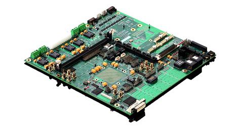
I. MID three-dimensional substrates and traditional flat circuit boards PCB
The design and manufacturing of electronic products are moving towards being thin, short and small, and circuit boards are also clearly developing towards fine lines and multi-layers. In terms of the control of the volume of finished products, space saving and rationalization are emphasized.
Based on the technical considerations of easy assembly and easy wiring, the three-dimensional substrate (MID) that came out as early as 1987 is expected to be more popular in the future. MID is the abbreviation of Molded Interconnect Device, which means molded interconnect components. It is a plastic injection-molded part with a three-dimensional wire loop on the surface; representative examples in the industry include hidden antennas in mobile phones that are not exposed, and LED light-emitting parts of famous Japanese watches, etc., mainly for its advantages of saving space, easy assembly, and high yield.
Similarly, in order to be thin, light and short, the general traditional flat printed circuit board PCB has evolved from double-sided board, four-layer board (PC motherboard), six-layer board, eight-layer board, twelve-layer board, and even developed to HDI (High Density Interconnect) high-density interconnect technology multi-layer board, line width / line spacing L / S (Line / Space) even to 2 / 2 (Mils), that is, 50 microns of fine lines, so as to meet the increasing requirements of IC chip packaging pins. Mainly used for information and communication products motherboard. In a finished product, the above two uses are sometimes complementary.
2.Manufacturing method of three-dimensional substrate MID
The manufacturing method of MID three-dimensional substrate is basically divided into film method (FILM TECHNIQUE, there are three categories:
CAPTURE PROCESS, TRANSFER PROCESS, HOT STAMPING, etc.), that is, the conductive material is made into individual soft films, and then attached to the injection mold plastic by one of the above three methods.
There is also There are three types of molding: one-shot molding, PHOTOIMAGIING image transfer method, and secondary molding.
For one-shot molding, PHOTOIMAGIING image transfer method, the process adopts electroplating grade resin injection molding, such as PES, LCP liquid crystal resin, epoxy resin, SPS, etc., through roughening, catalyst coating, chemical copper, electroplating photoresist (EDPR), exposure and development, electroplating, etching, stripping, and electroplating.
There are two types of secondary molding methods, PCK and SKW. First, electroplating grade resin is used for one-shot molding, and then roughening, catalyst coating, secondary molding, roughening, chemical copper, and electroplating are used.
The one-shot molding image transfer method has better molding properties and circuit thinning.
At present, MID is also promising in IC packaging, MCM packaging, LED CASE connectors, crystal vibration CASE, and various EMI electromagnetic wave protection parts. There are many mass production companies in Japan. Taiwan’s professional MID factories are in the embryonic stage. A few companies are entering the field of electroplating photoresist with electroplating coating technology, and then combined with plastic injection, electroplating and the most important subject-customer research and development.
3.Introduction to electrophoretic photoresist method
PCB printed boards are printed by screen (no exposure), dry film (DRY FILM) photoresist, wet film (WET OR LIQUID) photoresist, electrophoretic photoresist (EDPR) according to the thickness of the circuit. The film thickness is getting thinner and thinner, and the positive photoresist is only 6 microns. The line width and line spacing that can be made are also getting smaller and smaller, which can be used as the inner layer of precision PCB, BGA and other purposes.
Among the above methods, only EDPR can make 3D Three-dimensional uniform coating.
Electrophoretic coating is generally called electrophoretic coating in Taiwan or Japan. If the coating contains a photosensitive agent and is sensitive to ultraviolet light UV, it is an electrophoretic photoresist, which has two types: positive and negative photoresists. Positive photoresists are decomposed by UV exposure, so positive photoresists are preferred when there are finer through holes (PTH). Since three-dimensional plastic products need to be exposed, there are restrictions on the exposure height difference (or less than 3 mm), PTH (above 0.8 mm) line thickness, etc.
Positive and negative electrophoretic photoresists developed in Japan and Taiwan are mostly acrylic resins, while the United States has PU series positive photoresists.
The main difference between acrylic series electrophoretic photoresists and general cathode epoxy resin electrophoretic coatings is that the viscosity is higher, so the operating solid content is lower, and the pre-treatment of the board is more stringent.
The manufacture of MASK (mask) is the focus of this method. It is necessary to make a film that meets the requirements of 3D exposure.
The entire MID The electrophoretic photoresist process, as mentioned above, is roughly as follows: 1. Electroplating grade resin injection molding, such as PES, LCP liquid crystal resin, epoxy resin, SPS, etc., 2. Roughening, catalyst coating, chemical copper, 3. Electrodeposition photoresist (EDPR), 4. Exposure and development, 5. Electroplating Ni/Pb, Ni/Au, 6. Stripping, etching, and so on. There are about six steps.
Positive and negative photoresists are slightly different. This EDPR method can be used on finer circuits.
4. Future potential of MID
Currently, Germany, Japan, and the United States are the main countries for MID research and development. Japan’s development is mostly used for the thinness, shortness and special functions of traditional circuit boards PCB. Germany’s research and development of 3D-MID is used for larger parts such as automotive control engineering, emphasizing 1. Design freedom, mechatronics, miniaturization, new functions, and multi-type. 2. Rationalization, fewer parts, fewer processes, fewer materials, and high reliability 3. Environmentally friendly, uniform materials, recyclable, less materials, and harmless disposal. The annual growth rate in recent years has been above 25%, and future growth is expected.