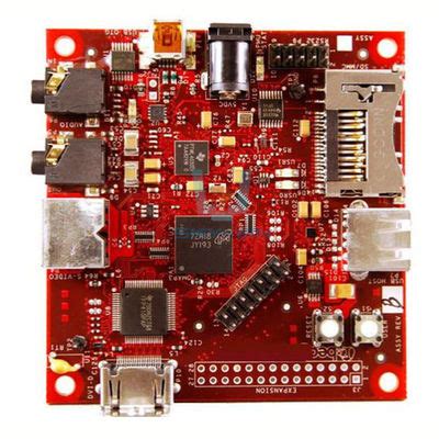
Importance of electroplating to printed circuit boards
On printed circuit boards, copper is used to interconnect components on the substrate. Although it is a good conductor material for forming the conductive path pattern of the printed circuit board, it is easy to lose its luster due to oxidation and lose its solderability due to corrosion if exposed to air for a long time. Therefore, various technologies must be used to protect copper traces, vias and plated through holes, including organic coatings, oxide films and electroplating technologies.
Organic coatings are very simple to apply, but they are not suitable for long-term use due to changes in their concentration, composition and curing cycle, and they may even cause unpredictable deviations in solderability. Oxide films can protect circuits from corrosion, but they cannot maintain solderability. Electroplating or metal coating processes are standard operations to ensure solderability and protect circuits from corrosion, and play an important role in the manufacture of single-sided, double-sided and multi-layer printed circuit boards. In particular, plating a layer of solderable metal on the traces has become a standard operation to provide a solderability protective layer for copper traces.
The interconnection of various modules in electronic equipment often requires the use of printed circuit board plug sockets with spring contacts and printed circuit boards with connecting contacts designed to match them. These contacts should have high wear resistance and low contact resistance, which requires plating a layer of rare metal on them, the most commonly used metal being gold. In addition, other coating metals can be used on the printed wires, such as tin plating, tin plating, and sometimes copper plating in certain printed wire areas.
Another coating on copper printed wires is organic, usually a solder mask, and a layer of epoxy resin film is applied by screen printing technology in areas where soldering is not required. This process of applying a layer of organic solder preservative does not require electronic exchange. When the circuit board is immersed in a chemical plating solution, a nitrogen-tolerant compound can adhere to the exposed metal surface and will not be absorbed by the substrate.
The sophisticated technology and strict requirements for environmental and safety adaptability required for electronic products have led to great progress in electroplating practice, which is clearly reflected in the manufacturing of high-complexity, high-resolution multi-substrate technology. Electroplating has reached a high level through the development of automated, computer-controlled electroplating equipment, the development of highly complex instrumentation for chemical analysis of organic and metal additives, and the emergence of technologies for precise control of chemical reaction processes.
There are two standard methods for growing metal layers in circuit board conductors and through holes: line plating and full-board copper plating, which are described as follows.
1.Line plating
In this process, only the areas where circuit patterns and through holes are designed receive copper layer formation and etch resist metal plating. During the line plating process, the increased width of each side of the line and pad is roughly equivalent to the increased thickness of the electroplated surface, so it is necessary to leave a margin on the original film.
In line plating, basically most of the copper surface must be masked with resist, and electroplating is only performed where there are circuit patterns such as lines and pads. Since the surface area to be plated is reduced, the required power supply current capacity is usually greatly reduced. In addition, when using contrast reverse photopolymer dry film plating resist (the most commonly used type), its negative film can be made with a relatively inexpensive laser printer or plotter. The anode consumes less copper in the circuit plating, and less copper needs to be removed during the etching process, thus reducing the analysis and maintenance costs of the electrolytic bath. The disadvantage of this technology is that the circuit pattern needs to be plated with tin/lead or an electrophoretic resist material before etching, which is removed before the solder resist is applied. This increases the complexity and adds an additional set of wet chemical solution processing.
2.Full board copper plating
In this process, the entire surface area and drilled holes are copper plated, some resist is poured on the unwanted copper surface, and then the etching resist metal is plated. Even for a medium-sized printed circuit board, this requires an electroplating that can provide a considerable current to produce an easy-to-clean, smooth, bright copper surface for subsequent processing. If there is no photoplotter, a negative film is needed to expose the circuit pattern, making it a more common contrast reversal dry film photoresist.
Etching a fully copper-plated circuit board will remove most of the plated material on the circuit board again, and the burden of additional corrosion on the anode is greatly increased due to the increase in the copper carrier in the etchant. Figure 8-1 shows the printed circuit board electroplating process flow chart for the stripping process. For the manufacture of printed circuit boards, circuit plating is a better method, and its standard thickness is as follows:
1) Copper
2) Tin-lead (circuit, pad, through hole)
3) Nickel 0.2mil
4) Gold (connector top) 50μm The reason for maintaining such parameters in the electroplating process is to provide the metal plating with high conductivity, good solderability, high mechanical strength and ductility required to withstand component terminal panels and copper filling from the circuit board surface to the plated through hole.