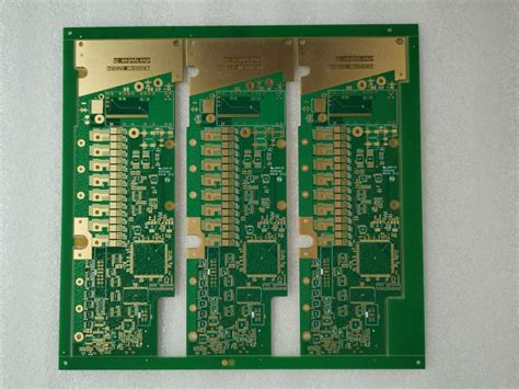
Optimizing Multi-Layer PCB Assembly for Enhanced Performance
Key Takeaways
Effective multi-layer PCB assembly requires a holistic approach that balances technical precision with strategic material selection. Modern high-density interconnect (HDI) designs demand rigorous attention to dielectric properties and thermal expansion coefficients when choosing substrate materials. PCBA specialists increasingly favor low-loss laminates with stable glass transition temperatures (Tg) to maintain signal integrity across multiple layers.
"Proper layer stacking sequence optimization can reduce impedance mismatches by up to 40% in complex PCB assembly projects," notes a leading electrical engineer from IPC’s technical committee.
Three critical success factors emerge for multi-layer PCB manufacturing:
- Z-axis expansion control through compatible material pairings
- Laser-drilled microvia implementation for vertical interconnects
- Sequential lamination protocols for stress distribution
Advanced PCBA workflows now incorporate real-time thermal imaging during press cycles to validate layer alignment accuracy. This prevents delamination risks in designs exceeding 12 layers while maintaining ±25µm registration tolerances. For high-frequency applications, mixed dielectric stacking techniques help manage electromagnetic interference without compromising board thickness targets.
Tip: Implement cross-sectional analysis after first-article inspection to verify interlayer resin flow patterns in your PCB assembly process.
Recent advancements in direct imaging systems and automated optical inspection (AOI) have revolutionized defect detection capabilities. These technologies enable <25µm feature verification across all conductive layers, particularly crucial for via-in-pad configurations in PCBA designs. Manufacturers report 68% reduction in cross-talk incidents when combining optimized layer sequencing with grounded coplanar waveguide structures.
Transitioning to volume production requires careful evaluation of panel utilization rates and laser ablation parameters. Leading contract manufacturers achieve 92% first-pass yield rates through:
- Dynamic thermal profiling of reflow processes
- Ionic contamination testing post-surface finishing
- Time-domain reflectometry for impedance validation
As multi-layer PCB complexity increases, adopting model-based definition (MBD) frameworks ensures seamless data transfer between design and assembly stages. This approach reduces interpretation errors in layer-specific requirements while maintaining compliance with IPC-2221B standards for high-reliability electronics.
Material Selection Strategies for High-Performance Multi-Layer PCBs
Effective PCB assembly begins with strategic material selection, a critical factor influencing signal integrity, thermal stability, and long-term reliability in multi-layer PCBs. The choice of substrate, conductive layers, and dielectric materials directly impacts operational efficiency and manufacturing yield, particularly in high-frequency or high-power applications.
For PCBA projects requiring enhanced thermal performance, materials like polyimide or Rogers 4350B laminates are preferred for their low dielectric loss and high glass transition temperatures (Tg > 280°C). These substrates minimize signal attenuation in high-speed circuits while resisting warping during reflow soldering. In contrast, standard FR-4 remains cost-effective for consumer electronics but requires careful evaluation of its coefficient of thermal expansion (CTE) to prevent layer delamination in dense multi-layer stacks.
| Material Type | Thermal Conductivity (W/m·K) | Dk (1 GHz) | Typical Applications |
|---|---|---|---|
| FR-4 | 0.25 | 4.5 | Consumer electronics |
| Polyimide | 0.45 | 3.5 | Aerospace, military |
| Rogers 4350B | 0.62 | 3.48 | RF/mmWave systems |
| Ceramic-filled PTFE | 0.85 | 2.94 | 5G infrastructure |
Copper foil selection further refines performance: low-profile rolled copper improves etching precision for fine-pitch traces, while electrodeposited copper offers higher ductility for multi-layer PCB assembly requiring complex via structures. Adhesive systems must also align with thermal profiles; epoxy-based prepregs with <1% resin flow ensure uniform bonding without impeding impedance control.
Three key considerations govern material optimization:
- Signal loss tolerance: High-frequency designs demand substrates with stable dissipation factors (Df) across temperature gradients.
- Thermal cycling resilience: Materials with CTE < 14 ppm/°C prevent interfacial stress in boards exceeding 12 layers.
- Manufacturing compatibility: Prepreg curing times and lamination pressures must align with PCBA facility capabilities to avoid voids or misregistration.
By balancing these parameters, engineers mitigate risks like electromigration or delamination, ensuring robust performance in mission-critical multi-layer PCB assemblies.
Precision Layer Stacking Techniques to Improve Signal Integrity
Effective multi-layer PCB assembly relies on meticulous layer stacking strategies to mitigate signal degradation in high-speed circuits. At the core of this process lies the strategic arrangement of power, ground, and signal layers, which directly influences impedance control and electromagnetic interference (EMI) reduction. Modern PCBA designs often employ sequential lamination methods, where alternating prepreg and copper layers are bonded under precise temperature and pressure conditions to minimize air gaps and ensure uniform dielectric properties.
A critical consideration involves optimizing the dielectric constant (Dk) of insulating materials to maintain consistent signal propagation speeds across layers. For instance, using low-loss laminates like Rogers 4350B in high-frequency applications reduces phase distortion, while symmetrical layer stacking balances thermal stresses during reflow soldering. Engineers frequently implement embedded capacitance layers near power planes to suppress voltage fluctuations, a technique proven to enhance signal-to-noise ratios in dense PCB assembly layouts.
Advanced registration systems play a pivotal role in aligning layers with sub-25μm accuracy, particularly for designs requiring microvia-in-pad structures or HDI (high-density interconnect) routing. Automated optical inspection (AOI) systems validate layer alignment post-lamination, preventing misregistration-induced defects like annular ring fractures. Additionally, incorporating ground shielding layers between high-speed signal traces minimizes crosstalk—a common challenge in 12+ layer PCBA configurations.
To further refine signal integrity, designers adopt controlled impedance routing rules tailored to each layer’s function. For example, stripline configurations in internal layers provide superior EMI shielding compared to surface-level microstrip traces. Thermal simulation tools are increasingly integrated into stacking workflows to predict warpage risks, ensuring mechanical stability across operational temperature ranges—a vital step for aerospace and automotive multi-layer PCB assemblies.
By harmonizing material science, precision manufacturing, and simulation-driven design, these techniques elevate the reliability of complex PCB assembly projects while aligning with scalable production frameworks. This foundational approach seamlessly transitions into addressing thermal management challenges, another critical pillar of high-performance multi-layer board design.
Thermal Management Solutions for Dense Multi-Layer PCB Designs
Effective thermal management is critical in multi-layer PCB assembly designs, particularly as component density increases and power demands escalate. Modern PCBA configurations often integrate high-speed processors, power modules, and RF components, which generate significant heat. Without proper dissipation, thermal stress can degrade signal integrity, warp substrates, and reduce operational lifespan.
A primary strategy involves selecting materials with high thermal conductivity. For instance, using metal-core substrates or ceramic-filled laminates enhances heat transfer away from critical components. In PCB assembly, embedding thermally conductive adhesives between layers helps distribute heat more evenly, preventing localized hotspots. Additionally, strategic placement of thermal vias—plated holes filled with conductive epoxy—creates vertical pathways to channel heat toward external heatsinks or copper planes.
Layer stacking methodologies also play a role. Pairing high-power layers with adjacent ground planes improves heat dissipation while maintaining electromagnetic shielding. Advanced PCBA designs often incorporate asymmetric stack-ups, placing power-intensive layers closer to the board’s exterior for improved airflow exposure. Computational fluid dynamics (CFD) simulations are increasingly used to model airflow patterns and optimize component placement for passive cooling.
For densely packed designs, active cooling solutions like micro-fans or thermoelectric coolers (TECs) may supplement passive methods. However, these require careful integration to avoid mechanical interference with multi-layer PCB assembly tolerances. Designers must also account for coefficient of thermal expansion (CTE) mismatches between materials, which can induce mechanical stress during temperature cycling.
Finally, post-assembly validation through infrared thermography ensures thermal management systems perform as intended. By balancing material innovation, layout optimization, and validation protocols, engineers can achieve reliable thermal performance even in the most complex PCBA environments.
Advanced Via-in-Pad and Microvia Integration Best Practices
The evolution of multi-layer PCB assembly demands meticulous attention to interconnect architectures, particularly when integrating via-in-pad (VIP) and microvia technologies. These methods address the challenges of high-density component placement and signal integrity preservation in modern PCBA designs, enabling engineers to optimize space utilization while maintaining electrical performance.
Via-in-pad techniques eliminate the need for dedicated via keep-out zones by placing vias directly under component pads, reducing trace lengths and minimizing parasitic inductance. This approach is particularly advantageous for ball grid array (BGA) and quad flat no-lead (QFN) packages, where pad real estate is limited. However, successful implementation requires precise control over laser drilling tolerances and copper plating uniformity to prevent voids or uneven solder joint formation. For high-frequency PCB assembly, filling vias with conductive epoxy or copper paste further enhances thermal dissipation and mechanical stability.
Microvias, defined by their aspect ratios below 1:1, enable vertical interconnects in HDI (high-density interconnect) PCBA without compromising layer stacking precision. Staggered microvia configurations outperform stacked variants by reducing stress concentration points, a critical factor for thermal cycling resilience. When paired with sequential lamination processes, these structures support impedance-controlled routing for high-speed differential pairs while mitigating crosstalk risks.
Key design considerations include:
- Pad geometry optimization to accommodate viaicking
- Plating thickness consistency (targeting 25–30 μm for reliability)
- Thermal relief strategies for components with high power dissipation
In manufacturing, automated optical inspection (AOI) systems must verify microvia alignment accuracy within ±15 μm tolerances, while cross-sectional analysis ensures void-free via fills. For prototype PCB assembly, employing laser-direct imaging (LDI) enhances pattern registration precision, reducing rework rates in complex stack-ups.
As multi-layer PCBA scales toward 20+ layers, combining VIP and microvia technologies with embedded passive components creates synergies that elevate both performance and miniaturization. By adhering to IPC-6012 Class 3 standards for via reliability and implementing design-for-manufacturing (DFM) checks early, teams can avoid delamination risks and achieve first-pass success rates exceeding 92% in high-mix production environments.
This progression in interconnect methodology directly supports the broader objectives outlined in thermal management and signal integrity sections, forming a cohesive framework for next-generation PCB assembly excellence.
Design Considerations for Reducing Crosstalk in Complex PCB Assemblies
In high-density multi-layer PCB assembly designs, crosstalk mitigation requires a systematic approach to layout optimization and signal management. Electromagnetic interference (EMI) between adjacent traces becomes a critical challenge as circuit densities increase, particularly in PCBA configurations with impedance-controlled routing and mixed-signal components.
A primary strategy involves optimizing trace spacing and orientation. Maintaining 3W spacing (three times the trace width) between parallel conductors significantly reduces capacitive coupling. For differential pairs, symmetrical routing with consistent intra-pair spacing minimizes skew while preserving signal integrity. Implementing ground planes between active signal layers in multi-layer stack-ups creates natural shielding, effectively isolating high-frequency signals from sensitive analog circuits.
Advanced PCB assembly workflows now integrate frequency-domain simulation tools to predict crosstalk hotspots during the design phase. By analyzing S-parameters and cross-talk coefficients, engineers can adjust trace geometries or insert guard traces before finalizing the layout. In mixed-signal PCBA designs, separating digital and analog power domains through split planes or moating techniques prevents noise propagation across functional blocks.
Material selection plays a dual role in crosstalk reduction. Low-Dk substrates with controlled dielectric constants minimize signal distortion, while high-Tg laminates maintain stable electrical properties under thermal stress. For ultra-high-speed designs in multi-layer PCB assemblies, embedded passives and coplanar waveguide structures offer superior EMI suppression compared to traditional microstrip configurations.
Transition management between layers demands careful via placement. Staggering blind vias and buried vias prevents vertical coupling paths, with back-drilling of unused via stubs becoming essential for GHz-range signals. In PCBA implementations using via-in-pad technology, non-conductive fill materials help mitigate impedance discontinuities that could exacerbate crosstalk.
Recent innovations in PCB assembly processes incorporate adaptive impedance tuning during manufacturing. Laser-trimmed resistors and programmable termination networks compensate for parasitic effects identified during time-domain reflectometry (TDR) testing. For mission-critical applications, active cancellation circuits using anti-phase signals provide dynamic crosstalk suppression in real-time operating conditions.
Validation protocols for crosstalk-optimized PCBA designs now combine eye diagram analysis with bit error rate testing (BERT), ensuring compliance with industry standards like IPC-2221B and JESD51-14. These measures create robust foundations for next-generation electronics requiring both miniaturization and electromagnetic compatibility in complex multi-layer architectures.
Reliability Testing Protocols for Multi-Layer Circuit Board Durability
Ensuring long-term durability in multi-layer PCB assembly requires systematic validation through industry-standard reliability tests. These protocols evaluate how PCBA designs withstand operational stresses, environmental factors, and aging effects. A comprehensive testing regimen typically begins with thermal cycling assessments, where boards undergo repeated temperature fluctuations (-40°C to 125°C) to simulate real-world thermal expansion mismatches. This exposes weaknesses in PCB assembly materials, such as delamination risks in high-density interconnects or solder joint fatigue.
Accelerated life testing (ALT) further validates performance under extreme conditions, including elevated humidity (85% RH) and prolonged high-voltage exposure. For mission-critical applications, interconnect stress testing (IST) measures the mechanical stability of microvias and plated through-holes, ensuring signal integrity remains intact after 1,000+ cycles. Advanced labs employ scanning acoustic microscopy (SAM) to non-destructively inspect layer adhesion quality, identifying voids or resin-rich areas that could compromise multi-layer PCBA reliability.
To align with automotive or aerospace standards, vibration and shock testing replicate mechanical stresses encountered during operation. Boards mounted in test fixtures undergo frequency sweeps (5Hz–2kHz) and peak acceleration loads (up to 50G) to detect solder cracks or component displacement. Concurrently, electrical continuity monitoring tracks resistance changes in critical traces, highlighting potential opens or shorts.
Best practices mandate combining these physical tests with predictive failure modeling. Finite element analysis (FEA) simulates stress distribution across layers, guiding design optimizations for PCB assembly processes. Post-test failure analysis, using cross-sectioning and energy-dispersive X-ray spectroscopy (EDS), pinpoints root causes—whether material degradation, improper lamination, or insufficient via fill.
Implementing these protocols not only meets IPC-6012 and MIL-PRF-31032 compliance but also reduces field failure rates by up to 40%. As PCBA designs grow denser, integrating automated optical inspection (AOI) during testing phases enhances defect detection for micro-BGA packages and buried capacitors. This data-driven approach ensures multi-layer boards deliver consistent performance across their lifecycle, bridging the gap between prototyping and scalable production.
By prioritizing rigorous reliability validation, manufacturers mitigate risks in high-stakes applications while maintaining alignment with evolving PCB assembly quality benchmarks. This foundational testing phase directly supports subsequent discussions on cost-effective scaling and defect prevention in complex HDI layouts.
Cost-Effective Methods for Scaling Multi-Layer PCB Production
Achieving scalability in multi-layer PCB assembly requires balancing technical precision with economic efficiency. One pivotal approach involves adopting design-for-manufacturability (DFM) principles early in the development cycle. By collaborating with PCBA partners to standardize layer stack-ups and material specifications, manufacturers can reduce prototyping iterations and minimize material waste. For instance, consolidating dielectric materials with compatible thermal expansion coefficients across layers simplifies lamination processes, lowering per-unit costs at higher volumes.
Leveraging automated optical inspection (AOI) systems paired with predictive analytics optimizes quality control without inflating labor expenses. These systems detect defects like misaligned vias or incomplete solder joints during PCB assembly, preventing costly rework in later stages. Additionally, implementing panelization strategies—such as arranging multiple boards on a single panel—maximizes substrate utilization, particularly when working with high-cost materials like Rogers or polyimide.
Strategic supplier partnerships further enhance cost efficiency. Bulk purchasing of high-frequency laminates or low-loss prepregs often secures volume discounts, while standardized component libraries reduce procurement lead times. For PCBA workflows, modular tooling designs allow rapid reconfiguration between product variants, minimizing downtime during batch transitions.
Thermal management, a recurring challenge in multi-layer designs, can be addressed cost-effectively through embedded copper coins or selective via filling. These methods eliminate the need for external heat sinks in many applications, reducing both part counts and assembly complexity. When combined with simulation-driven design tools to predict thermal hotspots layouts virtually before committing to physical prototypes.
Finally, scaling production demands rigorous process standardization. Documenting every parameter—from lamination pressure profiles to solder paste application thickness—ensures consistency across manufacturing shifts. This practice not only streamlines PCB assembly but also simplifies compliance with automotive or aerospace certifications, which often require traceable process records. By integrating these strategies, manufacturers can achieve economies of scale without compromising the signal integrity or reliability inherent to advanced multi-layer architectures.
Avoiding Common Defects in High-Density Interconnect PCB Assembly
Achieving defect-free outcomes in high-density interconnect (HDI) PCB assembly requires meticulous attention to design, material compatibility, and process controls. As PCBA designs grow more complex with shrinking trace widths and tighter component spacing, manufacturers must address signal integrity risks, thermal stress points, and mechanical instability proactively.
One prevalent challenge in multi-layer PCB assembly is microcrack formation during thermal cycling. This often stems from mismatched coefficients of thermal expansion (CTE) between copper traces and substrate materials. Implementing low-CTE dielectrics and optimizing reflow soldering profiles can mitigate this risk. For instance, using glass-reinforced epoxy laminates (FR-4 with high Tg) instead of standard FR-4 improves dimensional stability under temperature fluctuations.
Another critical area is delamination in HDI PCBA, typically caused by inadequate lamination pressure or moisture absorption in prepreg layers. Adopting vacuum-assisted lamination and pre-baking moisture-sensitive materials ensures uniform layer adhesion. Additionally, laser-drilled microvias with aspect ratios below 1:1 reduce the likelihood of incomplete plating, a common defect in ultra-fine interconnects.
Electroplating voids in through-holes and vias remain a persistent issue. To address this, manufacturers are shifting toward pulse plating techniques, which enhance copper deposition uniformity in high-aspect-ratio structures. Pairing this with automated optical inspection (AOI) systems enables real-time detection of plating defects before final assembly.
Signal integrity challenges, such as impedance mismatches and crosstalk, escalate in dense multi-layer PCB assemblies. Employing controlled impedance routing and ground-shielding techniques between adjacent signal layers minimizes electromagnetic interference. For example, embedding buried capacitance layers within the stack-up can stabilize power delivery networks while reducing noise coupling.
Finally, solder bridging in fine-pitch components demands precision in PCBA stencil design and solder paste application. Using laser-cut stencils with trapezoidal apertures improves paste release consistency, while 3D solder paste inspection (SPI) systems verify deposition accuracy down to ±10μm. Integrating these strategies with design for manufacturability (DFM) checks ensures alignment between layout decisions and process capabilities, effectively reducing rework rates in high-density PCB assembly.
Conclusion
The evolution of multi-layer PCB assembly represents a critical juncture in modern electronics manufacturing, where precision and foresight directly translate to operational excellence. As industries demand higher circuit density and faster signal processing, optimizing PCBA workflows becomes indispensable for achieving reliability and thermal resilience in complex designs. By integrating advanced material selection, meticulous layer stacking, and innovative via-in-pad architectures, manufacturers can address signal degradation and heat dissipation challenges inherent to high-density layouts.
A holistic approach to PCB assembly prioritizes not only technical execution but also rigorous testing protocols. For instance, automated optical inspection (AOI) and thermal cycling tests ensure that multi-layer boards withstand real-world stressors while maintaining signal integrity. Furthermore, balancing cost-efficiency with quality requires adopting scalable production methods—such as panelization strategies—that minimize waste without compromising precision.
Ultimately, the success of multi-layer PCBA hinges on proactive design choices. Avoiding crosstalk through optimized trace routing and grounding techniques, coupled with strategic microvia placement, reduces post-production rework. As emerging technologies like 5G and IoT push the boundaries of circuit complexity, adhering to these principles will empower engineers to deliver robust, high-performance solutions that align with evolving industry standards.
FAQs
What distinguishes multi-layer PCB assembly from standard PCBA processes?
Multi-layer designs require precise layer stacking and advanced via-in-pad integration to maintain signal integrity, unlike single/double-layer boards. The complexity demands stricter thermal management and material selection to prevent delamination or warping during lamination.
How does material optimization impact the reliability of multi-layer PCBs?
High-performance substrates like low-loss dielectrics reduce signal attenuation, while copper foils with optimal thickness enhance current-carrying capacity. Material choices directly affect thermal conductivity and mechanical stability, critical for high-density designs.
What are common challenges in thermal management for dense PCB assemblies?
Heat dissipation becomes critical in multi-layer configurations due to confined airflow. Solutions include thermal vias, metal-core substrates, and strategic placement of heat sinks. Poor thermal planning can lead to electromigration or component failure.
Why is crosstalk mitigation vital in complex PCB assembly?
Closely spaced traces in multi-layer boards increase electromagnetic interference risks. Techniques like ground plane shielding, differential signaling, and impedance matching minimize noise, ensuring signal fidelity in high-speed applications.
How do microvias enhance performance in high-density PCBA?
Microvias enable shorter interconnects between layers, reducing parasitic inductance and capacitance. Laser-drilled microvias also improve routing density, essential for HDI (High-Density Interconnect) designs requiring miniaturization.
What reliability tests are mandatory for multi-layer PCB assemblies?
Testing includes thermal cycling (-55°C to 125°C), vibration resistance checks, and high-potential (HiPot) testing. Environmental stress screening (ESS) validates performance under extreme humidity and temperature conditions.
Can cost-effective scaling compromise multi-layer PCB assembly quality?
Balancing cost and quality involves optimizing panel utilization, adopting automated optical inspection (AOI), and selecting certified suppliers. Standardizing layer stack-ups and avoiding over-engineering also reduce expenses without sacrificing reliability.
What design software tools support error-free multi-layer PCB assembly?
Platforms like Altium Designer and Cadence Allegro offer advanced features for signal integrity analysis and 3D stack-up visualization, reducing prototyping iterations and ensuring compliance with IPC-6012 standards.
Explore Customized Solutions for Your PCB Assembly Needs
For tailored strategies in multi-layer PCBA design and manufacturing, please click here to consult our engineering team.