Difficult Problems and Solutions for Printed Circuit Boards
Difficult Problems and Solutions for Printed Circuit Boards
1.Q: We have introduced the problem of pure resistance. There must be some resistors whose performance is exactly what we expected. What about the resistance of a wire?
A: It is different. You probably mean a wire or a conductive strip in a printed circuit board that acts as a wire. Since room temperature superconductors have not yet been invented, any metal wire acts as a low-resistance resistor (it also has the functions of capacitance and inductance), so its impact on the circuit must be considered.
2.Q: The resistance of a very short copper wire in a small signal circuit must not be important, right?
A: Let’s consider a 16-bit ADC with an input impedance of 5kΩ. Assume that the signal line to the ADC input is composed of a 10cm conductive strip on a typical printed circuit board (thickness 0.038mm, width 0.25mm). At room temperature, it has a resistance of about 0.18Ω, which is slightly less than 5kΩ×2×2-16, and will produce a gain error of 2LSB at full scale.
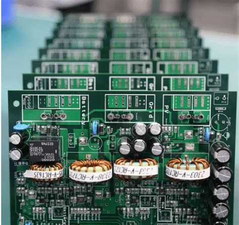
It can be shown that if the conductive strips of the printed circuit board are made wider (which is actually the case), the above problems may be alleviated. In analog circuits, it is usually better to use wider conductive strips, but many PCB designers (and PCB design programs) prefer to use the smallest width conductive strips to facilitate the layout of signal lines. In short, it is very important to calculate the resistance of the conductive strip and analyze its role in all possible problems.
3.Q: Will there be a problem with the capacitance formed by the conductive strip with too large width and the metal layer on the back of the printed circuit board?
A: The problem is very small. Although the capacitance formed by the conductive strip of the printed circuit board is important (even low-frequency circuits should be taken seriously because low-frequency circuits can also produce high-frequency parasitic oscillations), it should always be estimated first. If the above situation does not exist, even if the wider conductive strip forms a large capacitance, it will not cause problems. If it causes problems, a small area of the ground plane can be removed to reduce the capacitance to the ground.
4.Q: Let me leave this question for now! What is a ground plane?
A: If the copper foil on one side of a printed circuit board (or the entire interlayer of a multilayer printed circuit board) is used for grounding, then this is what we call a ground plane. Any ground line should be arranged to have the smallest possible resistance and inductance. If a system uses a ground plane, it is unlikely to be affected by ground noise. In addition, the ground plane also has the function of shielding and heat dissipation
5.Q: The ground plane mentioned here is difficult for manufacturers, right?
A: There were some problems in this regard 20 years ago. Today, due to the improvement of adhesives, solder resists and wave soldering technology in printed circuits, the manufacture of ground planes has become a routine operation for printed circuit boards.
6.Q: You said that a system using a ground plane is unlikely to be affected by ground noise. What ground noise problems are left that cannot be solved?
A: The basic circuit of a ground noise system has a ground plane, but its resistance and inductance are not zero – if the external current source is strong enough, it will affect the precision signal. This problem can be minimized by properly arranging the printed circuit board so that large currents cannot flow into areas that affect the ground voltage generated by precision signals. Sometimes breaks or slits in the ground plane can redirect large ground currents away from sensitive areas, but forced changes to the ground plane can also cause signals to bypass sensitive areas, so such process techniques must be used with caution.
7.Q: How can I know the voltage drop generated on a ground plane?
A: Usually the voltage drop can be measured, but sometimes it can be calculated based on the resistance of the ground plane material (nominal 1 ounce copper has a resistance of 0?45mΩ/□) and the length of the conductive strip through which the current passes, but the calculation may be complicated. Voltages in the DC to low frequency (50kHz) range can be measured using an instrument amplifier such as AMP?02 or AD620.
The amplifier gain is set to 1000 and connected to an oscilloscope with a sensitivity of 5mV/div. The amplifier can be powered by the same power supply as the circuit being tested, or by its own power supply. However, if the amplifier ground is separated from its power supply ground, the oscilloscope must be connected to the power supply ground of the power supply circuit used.
The resistance between any two points on the ground plane can be measured by adding a probe to these two points. The amplifier gain and oscilloscope sensitivity combine to achieve a measurement sensitivity of 5μV/div. The noise of the amplifier will increase the width of the oscilloscope waveform curve by about 3μV, but it is still possible to achieve a measurement resolution of about 1μV – this is enough to distinguish most ground noise, and the confidence level can reach 80%.
8.Q: What should be noted about the above test method?
A: Any alternating magnetic field will induce a voltage on the probe lead, which can be tested by short-circuiting the probes (and providing a bias current path to the ground resistance) and observing the oscilloscope waveform. The observed AC waveform is caused by induction, which can be reduced to a minimum by changing the lead position or trying to eliminate the magnetic field. In addition, it is also necessary to ensure that the amplifier ground is connected to the system ground. If the amplifier has this connection, there is no bias current return path and the amplifier cannot work. Grounding should also ensure that the grounding method used does not interfere with the current distribution of the circuit being tested.
9.Q: How to measure high-frequency ground noise?
A: It is difficult to measure high-frequency ground noise using a suitable wideband instrumentation amplifier, so it is more appropriate to use high-frequency and very high-frequency passive probes. It consists of a ferrite ring (outer diameter of 6 to 8 mm) with two coils on the ring, each with 6 to 10 turns. In order to form a high-frequency isolation transformer, one coil is connected to the input of the spectrum analyzer and the other coil is connected to the probe.
The test method is similar to the low-frequency case, but the spectrum analyzer uses an amplitude-frequency characteristic curve to represent the noise. This is different from the time domain characteristics, and the noise sources can be easily distinguished according to their frequency characteristics. In addition, the sensitivity of using a spectrum analyzer is at least 60dB higher than that of using a wideband oscilloscope.
10.Q: What is the inductance of the wire?
A: The inductance of the wire and the conductive strip of the printed circuit board cannot be ignored at higher frequencies. In order to calculate the inductance of the straight wire and the conductive strip, two approximate methods are introduced here.
For example, the inductance formed by a 1cm long and 0.25mm wide conductive strip is 10nH.
Wire inductance = 0.0002Lln2LR-0.75μH
For example: the inductance of a wire with a length of 1cm and an outer diameter of 0.5mm is 7.26nH (2R=0.5mm, L=1cm)
Conductive tape inductance = 0.0002Lln2LW+H+0.2235W+HL+0.5μH
For example: the inductance of a conductive tape on a printed circuit board with a length of 1cm and a width of 0.25mm is 9.59nH (H=0.038mm, W=0.25mm, L=1cm).
But the inductive reactance is usually
much smaller than the parasitic flux and induced voltage that cuts the inductive loop. The loop area must be minimized because the induced voltage is proportional to the loop area. This is easy to do when twisted pair wires are used for line wiring.
In printed circuit boards, the leads and return paths should be close together. Small wiring changes often minimize the impact, see source A coupled to low-energy loop B.
Reducing the loop area or increasing the distance between the coupled loops will minimize the effect. Usually the loop area is minimized and the distance between the coupled loops is increased as much as possible. Magnetic field shielding is sometimes needed, but it is expensive and prone to mechanical failure, so try to avoid it.
11.Q: In the “Application Engineer Q&A”, the non-ideal behavior of integrated circuits is often mentioned. It should be easier to use simple components such as resistors. Please explain the situation of close to ideal components.
A: I just hope that the resistor is an ideal component, but the short small cylinder at the end of the resistor lead acts just like a pure resistor. Real resistors also contain an imaginary resistance component – that is, a reactance component. Most resistors have a small capacitance in parallel with their resistance (typically 1 to 3pF). Although some thin film resistors are cut with spiral grooves in their resistive film, they are mostly inductive, with an inductive reactance of tens or hundreds of nanohenries (nH). Of course, wirewound resistors are generally inductive rather than capacitive (at least at low frequencies). After all, wirewound resistors are made of coils, so it is common for them to have an inductance of a few microhenries (μH) or tens of microhenries. Even so-called “inductance-free” wirewound resistors (where half the turns are wound clockwise and the other half are wound counterclockwise so that the inductances of the two halves cancel each other out) have a residual inductance of 1μH or more. For high-value wirewound resistors above about 10kΩ, the residual resistance is mostly capacitive rather than inductive, and the capacitance is as high as 10pF, which is higher than the capacitance of standard film or synthetic resistors. This reactance must be carefully considered when designing high-frequency circuits containing resistors.
12.Q: But many of the circuits you describe are used for precision measurements of DC or very low frequencies. Stray inductance and stray capacitance are not relevant in such applications, right?
A: Yes. Since transistors (either discrete transistors or transistors inside integrated circuits) have a wide bandwidth, oscillations may sometimes occur in the hundreds or thousands of megahertz band when the end of such a circuit is a reactive load. The offset and rectification associated with the oscillations can have a negative effect on low-frequency accuracy and stability.
Worse, such oscillations may not be visible on an oscilloscope, either because the oscilloscope bandwidth is too low compared to the bandwidth of the high-frequency oscillation being measured, or because the capacitance of the oscilloscope probe is sufficient to stop the oscillations. The best method is to use a wideband (low frequency to 1?5GHz or more) spectrum analyzer to check the system for parasitic oscillations. This check should be done when the input varies over the entire dynamic range, because parasitic oscillations sometimes appear in a very narrow range of the input frequency band.
13.Q: Are there any other questions about the resistance of resistors?
A: The resistance of resistors is not fixed, but varies with temperature. The temperature coefficient (TC) varies from a few ppm/°C (parts per million per degree Celsius) to thousands of ppm/°C. The most stable resistors are wirewound or metal film; the worst are composite carbon film.
A large temperature coefficient is sometimes useful (a previous Ask the Applications Engineer article mentioned how to use a +3500ppm/°C resistor to compensate for kT/q in the junction diode characteristic equation). But in general, the change in resistance with temperature can be a source of error in precision circuits.
If the accuracy of a circuit depends on matching two resistors with different temperature coefficients, then no matter how well they are matched at one temperature, they will not match at another. Even if the temperature coefficients of two resistors are matched, there is no guarantee that they will remain at the same temperature. Self-heating from internal power dissipation or external heat conducted from a heat source in the system can cause a temperature mismatch and thus resistance.
Even high-quality wirewound or metal film resistors can have a mismatch error of hundreds (or even thousands) of ppm/°C as a result of temperature. The obvious solution is to use two resistors that are manufactured so that they are very close to the same substrate, so that the system accuracy requirements are well matched at all times. This substrate can be the silicon wafer of a precision analog integrated circuit, or a piece of glass or metal film. Regardless of the substrate, the two resistors are well matched during manufacturing, have well-matched temperature coefficients, and are at nearly the same temperature (because they are so close together).