Application of TVS Devices in ESD Protection of Information Equipment
With the rapid development of electronic information technology, current semiconductor devices are increasingly miniaturized, high-density and multifunctional. In particular, applications such as fashionable consumer electronics and portable products that have strict requirements on the motherboard area are easily affected by electrostatic discharge (ESD).
The selection of circuit protection components is determined by the wiring conditions to be protected, the available circuit board space and the electrical characteristics of the protected circuit. Because the oxide layer in the IC circuit manufactured using advanced process technology is relatively thin, the gate oxide layer is more susceptible to damage. In addition, some complex semiconductor functional circuits using deep submicron processes and very fine line width wiring are more sensitive to the impact of circuit transient processes, which will aggravate the above problems. Therefore, the protection device must have a low clamping voltage to provide effective ESD protection; and a fast response time to meet the requirements of high-speed data lines; a high degree of package integration to suit the situation of tight printed circuit board surface for portable devices; at the same time, it must ensure that it will not deteriorate after multiple ESD processes to ensure the quality of high-end equipment. TVS (Transient Voltage Suppresser) was created to solve these problems, and it has become a key technical device for protecting electronic information equipment.
Characteristics and working principle of TVS
TVS is a new type of highly efficient circuit protection device that is widely used. It has an extremely fast response time (sub-nanosecond level) and a fairly high surge absorption capacity. When its two ends are subjected to a momentary high-energy impact, TVS can change the impedance value between the two ends from high impedance to low impedance at a very high speed to absorb a momentary large current, thereby clamping the voltage between its two ends to a predetermined value, thereby protecting the subsequent circuit components from the impact of transient high-voltage spike pulses.
Because of this, TVS can be used to protect equipment or circuits from static electricity, transient voltages generated when inductive loads are switched, and overvoltages generated by inductive lightning. Figure 1 shows the symbol and volt-ampere characteristic curve of TVS.
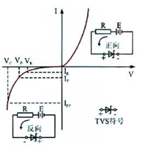
TVS tubes, like voltage regulator tubes, are also applied in reverse.
Among them, VR is called the maximum turning voltage, which is the critical voltage before reverse breakdown. VB is the breakdown voltage, and its corresponding reverse current IT is generally taken as 1 mA. VC is the maximum clamping voltage. When the peak current flowing through the TVS tube is the large current of IPP, the voltage across the tube will no longer rise. Therefore, the TVS tube can always limit the port voltage of the protected device or equipment within the effective range of VB~VC. Unlike the voltage regulator tube, the value of IPP can reach hundreds of amperes, while the clamping response time is only 1×10-12s. The maximum allowable pulse power of TVS is PM=VCIPP, and under a given maximum clamping voltage, the greater the power consumption PM, the greater its surge current tolerance.
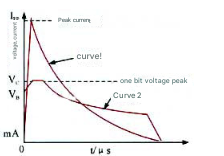
Figure 2 is the current and voltage waveform of the TVS tube observed on a dual-trace oscilloscope when it is subjected to a large current impact. In the figure, curve 1 is the current waveform in the TVS tube. It can be seen that: the current flowing through the TVS tube suddenly rises from 1mA to the peak value, and then decreases exponentially. Curve 2 is the voltage waveform at both ends of the TVS tube, which indicates that when the current in the TVS suddenly rises, the voltage at both ends of the TVS also rises. Under the action of the surge voltage, the voltage between the two poles of the TVS rises from the rated reverse shutdown voltage VRWM to the breakdown voltage VB and is broken down. With the emergence of breakdown current, the current flowing through TVS will reach the peak pulse current IPP, and the voltage at both ends will be clamped below the predetermined maximum clamping voltage VC. Afterwards, as the pulse current decays exponentially, the voltage between the two poles of TVS also decreases continuously during this process, and finally returns to the initial state. This is the process of TVS suppressing possible surge pulse power and protecting electronic components. In fact, when the two poles of TVS are subjected to reverse high-energy impact, it can change the impedance between the two poles from high to low at a speed of 10-12s to absorb surge power of up to several kilowatts, so that the potential between the two poles is clamped at a predetermined value, thereby effectively protecting the components in the electronic equipment from ESD damage.
Classification and selection method of TVS
TVS devices can be divided into unipolar and bipolar types according to polarity; they can be divided into general-purpose and special-purpose types according to their use; they can be divided into axial lead diodes, dual in-line TVS arrays, surface mount and high-power modules according to packaging and internal structure. The peak power of axial lead products can reach 400 W, 500 W, 600 W, 1500 W and 5 000 W. Among them, high-power products are mainly used in power feeders, and low-power products are mainly used in high-density installation occasions. For high-density installation occasions, dual-in-line and surface mount packaging forms can also be selected.
When selecting TVS, the following main factors should be considered:
(1) If the TVS may withstand peak pulse voltage (surge voltage) impact from two directions, bipolar should be selected, otherwise unipolar can be selected.
(2) The Vc value of the selected TVS should be lower than the maximum voltage of the protected component. Vc is the voltage of the diode in the cut-off state, that is, the voltage passing through the TVS in the ESD impact state. It cannot be greater than the tolerable limit voltage of the protected circuit, otherwise the device will be in danger of being damaged.
(3) The TVS should not be in a breakdown state under normal working conditions, and it is best to be below VR. The requirements of VR and VC should be considered comprehensively to select an appropriate TVS.
(4) If you know the more accurate surge current IPP, you can use VCIpp to determine the power; if you cannot determine the approximate range of IPP, it is better to use a TVS with a larger power. PM is the maximum peak pulse power dissipation value that TVS can withstand. Under a given maximum clamping voltage, the greater the power consumption PM, the greater its surge current tolerance; under a given power consumption PM, the lower the clamping voltage VC, the greater its surge current tolerance. In addition, the peak pulse power consumption is also related to the pulse waveform, duration and ambient temperature.
(5) The transient pulse that TVS can withstand is non-repetitive, and the pulse repetition frequency (ratio of duration to intermittent time) specified by the device is 0.01%. If repetitive pulses appear in the circuit, the accumulation of pulse power should be considered, otherwise the TVS may be damaged.
(6) For the protection of small current loads, a current limiting resistor can be consciously added to the circuit. As long as the resistance of the current limiting resistor is appropriate, it generally will not affect the normal operation of the circuit, but the current limiting resistor will greatly reduce the current generated by the interference. However, this may result in the selection of TVS tubes with lower peak power to protect low current load circuits.
(7) The capacitance C is determined by the cross section of the TVS avalanche junction, which is measured at a specific frequency of 1 MHz. The size of C is proportional to the current carrying capacity of the TVS. If C is too large, the signal will be attenuated. Therefore, C is an important parameter for selecting TVS for data interface circuits. For loops with higher data/signal frequencies, the capacitance of the diode will interfere with the circuit more, and the noise or attenuation of the signal strength will also be greater.
Therefore, the capacitance range of the selected device needs to be determined based on the characteristics of the loop. For high-frequency loops, the capacitance should generally be as small as possible (such as LCTVS, low-capacitance TVS, capacitance not greater than 3 pF), while for loops with low capacitance requirements, the capacitance can be selected to be higher than 40 pF.
(8) In order to meet the IEC61000-4-2 international standard, TVS diodes must be able to handle a minimum ESD shock of 8 kV (contact) and 15 kV (air). Some semiconductor manufacturers use higher shock resistance standards on their products. For some portable device applications with special requirements, designers can select devices as needed.
ESD protection based on TVS
The best way to deal with the damage of transient pulses to devices is to divert the transient current away from sensitive devices. The method is to connect the TVS diode in parallel with the protected circuit on the circuit board. In this way, when the transient voltage exceeds the normal working voltage of the circuit, the TVS diode will avalanche to provide an ultra-low resistance path for the transient current. As a result, the transient current is diverted through the diode, thereby avoiding the protected device and keeping the protected circuit at the cut-off voltage until the voltage returns to normal. When the transient pulse ends, the TVS diode automatically returns to the high-resistance state, and the entire circuit enters the normal voltage state.
Protection of the bottom connector of portable products
The bottom connector design factory is widely used in mobile consumer products. The current application products on the market are mainly portable products such as mobile phones, PDAs, DSCs (digital cameras) and MP3s. In these products, when the data line interface is connected to an external device, it may be subjected to high-energy impact, so the TVS bridge protection circuit shown in Figure 3 can be used. At present, common devices with integrated TVS and overcurrent protection functions include: NZQA series, MSQA series, NSQA series and SMF series. All of the above products have 4 single-phase independent line ESD protection. The package form of NZQA series is SOT-553, and the package form of the other three series is SC-88A. Since TVS devices in SOT5xx packages are all produced for 260℃ reflow temperature processing process, they meet 100% lead-free and electrostatic discharge protection requirements, thus reducing circuit board space by 36% and thickness by 40% compared with traditional packages. They are suitable for portable devices with strict requirements on circuit board space, such as mobile phones, digital cameras, MP3 players, etc.
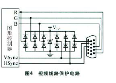
Protection of video lines
Video data lines have high data transmission rates (the data transmission rate is as high as 480 Mbps, and some video data transmission rates reach more than 1G), so low-capacitance LCTVS should be selected. Usually, a low-capacitance diode is connected in series with the TVS diode to reduce the capacitance of the entire line (can be less than 3 pF), so as to meet the requirements of high-speed loops. At present, the common video output port designs are D-SUB, DVI (28 lines), SCART (19 lines) and D-TERMINAL (mainly used in Japanese products). As shown in Figure 4, the ESD protection circuit of the D-SUB port video line.
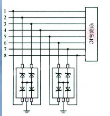
SIM card data line protection
SIM card data line protection has always been the focus of product design for various companies. When selecting devices for different purposes, it is necessary to avoid making the device work near the limit of its design parameters. It is also necessary to select devices with fast enough reaction speed and high enough sensitivity according to the characteristics of the protected circuit and the characteristics that may withstand ESD impact. This is very important for effectively playing the role of protection devices. In addition, devices with integrated other functions should also be given priority consideration. Figure 5 shows the SIM card data line protection circuit. Many recent new products are more adaptable to the high integration and miniaturization requirements of portable devices. Integrating ESD (TVS)/EMI/RFI protection in a chip device can not only effectively reduce space, but also greatly reduce device procurement costs and processing costs.
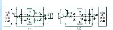
USB protection
Universal serial bus (USB) technology is a new way to connect PCs to different external devices. It can realize data exchange between the downstream port of PC, server, notebook and hub and the upstream port of peripheral end. The current USB technology has two data rates: low speed (1.5Mb/s) and full speed (12Mb/s). The 12Mb/s USB data stream is 10 times faster than the parallel port and 100 times faster than the standard serial port. The increase in frequency must be accompanied by devices that adapt to ESD sensitivity. Figure 6 shows a fast-response TVS application circuit that can meet the ESD protection of the USB line terminal and has good low-pass filtering function.
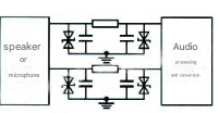
Audio, speaker data line protection
In terms of audio data line protection, the signal rate of the audio channel is relatively low and the requirements for capacitor devices are not too high (about 100 pF is acceptable). In fact, some mobile phone designs combine headphones and microphones, while others are discrete lines. In the former case, a single-channel TVS can be selected, while in the latter case, if the two circuits are adjacent, a multi-channel TVS array can be selected. In this way, only one device can be used to protect the two circuits. Figure 7 shows a protection circuit for an audio/speaker data line.
Button and switch protection
Since the data rate of the button and switch circuit is very low, there is no special requirement for the capacitance of the device, so an ordinary TVS array can be used.
PCB design and layout
PCB design considerations
For this design, the following points should be noted in PCB design:
(1) The more critical signal lines should be kept away from the protection circuit as much as possible, and the interfaces should be arranged on the same side as much as possible;
(2) Avoid connecting the protected circuit in parallel with the unprotected circuit. The interface signal line and the ground line should be directly connected to the protection device before entering the other parts of the circuit;
(3) The area surrounded by the loop formed by various signal lines and their feeders should be as small as possible to reduce radiation noise. If necessary, consider changing the position of the signal line or ground line;
(4) Keep the reset, interrupt, and control signals away from the input/output ports and away from the edge of the PCB;
(5) The use of highly integrated devices or diode arrays can not only greatly save space on the circuit board, but also reduce the parasitic line self-inductance that may be induced by the complexity of the circuit;
(6) Add grounding points wherever possible. The “one-point grounding” principle should be followed in circuit system design.
PCB layout
The most important thing about reasonable PCB layout is to avoid self-inductance while using TVS diode protection. ESD design is likely to cause parasitic self-inductance in the loop and form a strong voltage shock to the loop, which will cause the IC to withstand the limit and cause damage. The self-inductance voltage generated by the load is proportional to the intensity of the power supply change, and the transient characteristics of the ESD shock are very likely to induce high-strength self-inductance. The basic principle of reducing parasitic self-inductance is to shorten the shunt loop as much as possible. Therefore, all factors including the ground loop, the loop between the TVS and the protected circuit, and the path from the interface to the TVS must be considered. Therefore, only by placing the TVS device as close to the interface as possible and as close to the protected circuit as possible can the chance of self-inductance coupling to other adjacent circuits be reduced.
Conclusion
Using TVS to implement ESD protection for information equipment is a convenient, effective and reliable way. Compared with other components, TVS has its unique advantages. However, in specific applications, components should be selected according to different protection objects, and attention should be paid to the corresponding parameters and the different designs of each manufacturer. At the same time, optimized PCB design is also essential.