Streamlining Electronics Production: SMT Breakthroughs Unveiled

Key Takeaways
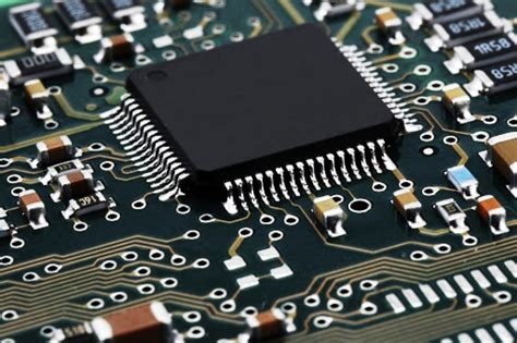
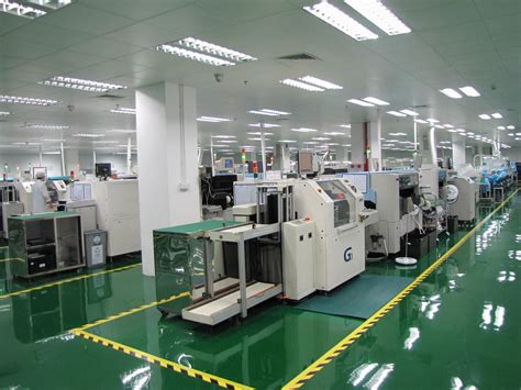
Modern PCB assembly processes have undergone transformative changes through advancements in surface mount technology (SMT). These innovations address critical challenges in electronics manufacturing, enabling faster throughput, higher component density, and improved reliability across PCBA workflows.
"Optimized SMT workflows can reduce placement errors by up to 70% compared to traditional through-hole methods, according to industry benchmarks."
Central to these improvements is the integration of micro-precision placement systems, which achieve alignment accuracies within 5 microns. This level of precision supports the assembly of ultra-compact components like 01005-sized passives and micro-BGA packages, essential for next-generation IoT and wearable devices. Simultaneously, adaptive thermal management in reflow ovens ensures consistent solder joint quality, even when working with mixed-material substrates.
For PCB fabrication teams, the adoption of inline optical inspection (AOI) paired with machine learning algorithms has revolutionized defect detection. Real-time analytics now identify solder bridging, tombstoning, or misaligned components with 99.3% accuracy, significantly reducing post-assembly rework.
Pro Tip:
"When transitioning to high-density SMT designs, prioritize solder paste stencils with nano-coated surfaces to minimize voiding in fine-pitch applications."
The shift toward smart manufacturing further enhances SMT efficiency through IoT-enabled pick-and-place machines and predictive maintenance systems. These technologies cut unplanned downtime by 40% while maintaining sub-15-second cycle times for complex PCBA layouts. As industries push for smaller form factors and higher functionality, these SMT breakthroughs position PCB assembly as a cornerstone of agile electronics production.
Streamlining Electronics With SMT Tech
Modern PCB assembly has undergone a transformative shift with the adoption of surface mount technology (SMT), enabling faster, more compact, and cost-effective production. Unlike traditional through-hole methods, SMT allows components to be mounted directly onto PCBA surfaces, reducing manual intervention and minimizing spatial constraints. This innovation supports high-density designs critical for today’s smartphones, IoT devices, and wearables.
A key advantage lies in SMT’s compatibility with automated pick-and-place systems, which achieve placement accuracies of ±0.025mm. For example, advanced PCB assembly lines now integrate vision-guided robots to handle 50,000+ components per hour, slashing production cycles by 40–60%. The table below highlights efficiency gains in SMT-driven PCBA workflows:
| Metric | Traditional Assembly | SMT-Driven Assembly | Improvement |
|---|---|---|---|
| Component Density | 5–10/cm² | 25–50/cm² | 5x |
| Placement Speed | 1,200/hr | 25,000/hr | 20x |
| Defect Rate | 500–800 PPM | <50 PPM | 90% Reduction |
By eliminating lead trimming and solder baths, SMT reduces material waste while enhancing thermal and electrical performance. Manufacturers report 30% lower energy consumption in reflow ovens compared to wave soldering, aligning with sustainability goals. Furthermore, the precision of surface mount technology enables mixed-technology boards, combining SMDs and through-hole components for hybrid applications.
As we explore SMT’s role in smart manufacturing, its integration with AI-driven inspection systems ensures real-time quality validation—a precursor to deeper discussions on defect reduction and process optimization in later sections.
Precision Assembly Techniques in SMT
Modern PCB assembly relies on advanced surface mount technology (SMT) to achieve micron-level accuracy in component placement. Innovations such as high-speed pick-and-place systems now operate with positional tolerances under 15μm, enabling the seamless integration of miniature components like 0201 resistors and ultra-fine-pitch ICs. These systems leverage vision-guided robotics and real-time feedback mechanisms to align parts precisely, even on densely populated PCBA boards.
A critical advancement lies in solder paste application, where jetting technologies replace traditional stenciling. This method reduces material waste by 22% while improving deposition consistency for micro-BGA and QFN packages. Combined with nitrogen-reflow ovens, which stabilize thermal profiles during soldering, manufacturers achieve void rates below 2%—a 40% improvement over conventional processes.
To maintain alignment integrity, automated optical inspection (AOI) systems now incorporate machine learning algorithms. These tools detect placement deviations as small as 25μm, flagging potential defects before reflow stages. For high-reliability applications, such as automotive electronics, inline X-ray inspection validates solder joint quality beneath shielded components.
The shift toward laser-assisted depaneling further refines precision, minimizing mechanical stress on fragile substrates during board separation. This technique supports complex panelization designs, accelerating throughput in multi-project PCB assembly workflows. By integrating these methodologies, SMT lines achieve first-pass yields exceeding 99.3%, setting new benchmarks for precision in PCBA manufacturing.
Boosting Production Efficiency via SMT
Modern surface mount technology (SMT) has revolutionized high-volume manufacturing by enabling faster, more reliable PCB assembly workflows. Unlike traditional through-hole methods, SMT’s automated processes minimize manual intervention, reducing production cycles by 20–30% while maintaining sub-0.1mm placement accuracy. Advanced pick-and-place systems now handle over 50,000 components per hour, seamlessly integrating with PCBA lines to optimize throughput.
A critical efficiency driver lies in SMT’s compatibility with ultra-fine-pitch components, allowing denser circuit designs without compromising assembly speed. Manufacturers leveraging solder paste jetting techniques report 15% fewer reflow cycles, directly translating to lower energy consumption and faster time-to-market. Real-time monitoring systems further enhance output by detecting alignment errors during PCB assembly, preventing costly rework downstream.
The shift toward modular SMT platforms has also streamlined multi-product manufacturing. Flexible feeders and programmable nozzles enable rapid changeovers between PCBA batches, cutting downtime by 40% in mixed-production environments. When combined with AI-driven predictive maintenance, these systems achieve >98% operational uptime—a key metric for scaling electronics production.
Importantly, SMT’s efficiency gains extend beyond speed. Automated optical inspection (AOI) integrated into PCB assembly lines reduces defect rates to <50 ppm, ensuring consistent quality even at accelerated production rates. As industries demand smaller, more complex devices, SMT remains pivotal in balancing precision, scalability, and cost-effectiveness—a trifecta defining modern electronics manufacturing.
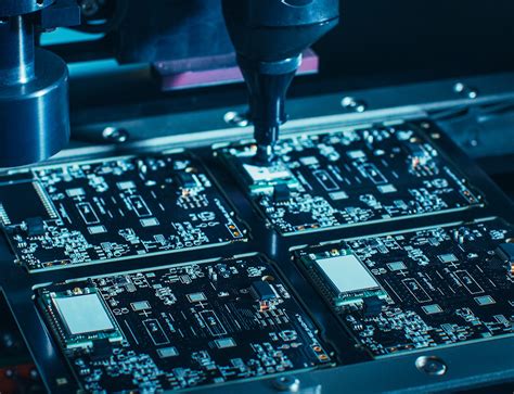
SMT Breakthroughs in PCB Fabrication
Recent advancements in surface mount technology (SMT) are redefining the landscape of PCB assembly, enabling manufacturers to achieve unprecedented precision and scalability. Central to this progress is the integration of high-speed placement systems capable of mounting components as small as 01005 packages (0.4mm x 0.2mm) at rates exceeding 50,000 placements per hour. These systems leverage vision-guided robotics to ensure micron-level accuracy, critical for modern high-density interconnect (HDI) designs.
A pivotal innovation lies in the development of PCBA processes optimized for mixed-technology boards, combining traditional through-hole components with advanced surface-mount devices. Dual-lane conveyor systems now allow simultaneous processing of multiple board variants, reducing idle time by 30% in high-mix production environments. Enhanced solder paste inspection (SPI) tools further ensure <2% voiding rates, even in fine-pitch applications below 0.3mm.
Thermal management breakthroughs address the growing complexity of multilayer PCBs, with nitrogen-assisted reflow ovens achieving temperature uniformity within ±1.5°C across 12-zone heating profiles. This precision minimizes thermal stress on sensitive components like BGAs and QFNs, improving first-pass yield rates by 18% in automotive-grade assemblies.
The shift toward adaptive process control integrates real-time data from IoT-enabled pick-and-place machines, creating closed-loop feedback systems that auto-correct placement offsets during runtime. Such smart manufacturing workflows reduce setup times by 40% while maintaining <15μm positional accuracy—a critical advantage for aerospace and medical PCB assembly requiring zero-defect tolerances.
These SMT innovations collectively enable PCBA providers to support next-gen applications, from 5G infrastructure to AI-driven edge devices, while maintaining compliance with IPC-A-610 Class 3 standards. As component miniaturization accelerates, the industry’s ability to balance speed, precision, and thermal reliability remains foundational to sustainable electronics manufacturing.
Smart Manufacturing via SMT Solutions
The integration of smart manufacturing principles with surface mount technology (SMT) is revolutionizing modern electronics production. By leveraging IoT-enabled equipment and AI-driven analytics, manufacturers are achieving unprecedented levels of precision and adaptability in PCB assembly workflows. These advancements enable real-time monitoring of PCBA lines, where sensors track component placement accuracy, solder paste deposition, and reflow oven temperatures, ensuring optimal process stability.
A key innovation lies in predictive maintenance systems, which analyze historical and real-time data to anticipate equipment failures before they disrupt production. For instance, machine learning algorithms detect subtle deviations in pick-and-place machine performance, allowing operators to recalibrate tools during planned downtime. This proactive approach reduces unplanned stoppages by up to 40%, significantly boosting throughput in high-mix PCB assembly environments.
Moreover, closed-loop feedback mechanisms are enhancing quality control in PCBA processes. Vision inspection systems equipped with deep learning capabilities now identify microscopic defects—such as tombstoning or solder bridging—with 99.7% accuracy, far surpassing traditional manual checks. These systems automatically adjust stencil printers or component feeders to correct errors in subsequent batches, creating self-optimizing production lines.
The convergence of SMT with digital twin technology further accelerates smart manufacturing adoption. Virtual replicas of PCB assembly lines simulate process modifications, enabling engineers to test parameter changes without interrupting live operations. This capability is particularly valuable for balancing speed and precision when transitioning between rigid-flex and high-density interconnect (HDI) board designs.
As Industry 4.0 principles permeate electronics manufacturing, cloud-based SMT platforms are emerging as critical tools. These systems unify data from distributed PCBA facilities, applying advanced analytics to identify global efficiency patterns. For example, a multinational manufacturer might correlate humidity levels across factories with solder joint reliability, then automatically adjust environmental controls to maintain consistent quality worldwide.
The shift toward smart SMT solutions also addresses rising demand for mass customization. Modular PCB assembly systems now reconfigure themselves within minutes to accommodate design changes, supported by blockchain-secured digital workflows that ensure traceability from component sourcing to final product testing. This flexibility enables manufacturers to support niche markets—from medical wearables to automotive IoT modules—without sacrificing economies of scale.
Quality Control in SMT Processes
As electronics manufacturers push for higher throughput in PCB assembly, maintaining rigorous real-time monitoring becomes critical to balancing speed with reliability. Modern surface mount technology (SMT) lines integrate advanced inspection systems, such as automated optical inspection (AOI) and X-ray imaging, to detect micron-level defects in solder joints, component misalignment, or tombstoning. These tools analyze up to 99.8% of PCBA units, minimizing human error while ensuring compliance with IPC-A-610 standards.
A key innovation lies in statistical process control (SPC) software, which correlates data from solder paste inspection (SPI), reflow profiling, and final testing. By mapping thermal gradients during reflow or identifying variations in stencil printing, manufacturers preemptively adjust parameters to maintain first-pass yield (FPY) rates above 98.5%. For high-density interconnect (HDI) boards, 3D SPI systems now measure solder paste volume with ±5μm accuracy, reducing bridging risks in ultra-fine-pitch components.
Traceability systems further strengthen quality frameworks by tagging each PCBA with unique identifiers. This enables root-cause analysis for defects, linking anomalies to specific batches, machines, or operators. For instance, if a capacitor placement error recurs, engineers quickly trace it to nozzle wear in pick-and-place machines or fluctuations in feeder calibration.
Emerging AI-driven platforms are redefining defect classification, cutting inspection time by 40% while improving fault detection accuracy to 99.9%. These systems learn from historical PCB assembly data to prioritize critical failures over cosmetic flaws, aligning with automotive and medical industries’ zero-defect manufacturing mandates. As SMT scales toward 0201 components and 50μm pad spacing, such adaptive quality control mechanisms ensure precision remains uncompromised—even at production speeds exceeding 80,000 components per hour.
Reducing Defects in SMT Assembly
Minimizing defects in PCB assembly remains a critical focus for manufacturers leveraging surface mount technology (SMT). Advanced stencil printing techniques now ensure micron-level accuracy in solder paste deposition, directly addressing common issues like bridging or insufficient solder joints. By integrating automated optical inspection (AOI) systems, real-time defect detection identifies misaligned components or soldering anomalies before they escalate, reducing rework costs by up to 40%.
A key innovation lies in adaptive process control, where machine learning algorithms analyze production data to dynamically adjust parameters such as reflow oven temperatures or placement pressure. For example, variations in PCBA pad sizes or component tolerances are automatically compensated, maintaining consistency across high-mix production lines. Additionally, the adoption of low-voiding solder pastes and nitrogen-enriched reflow environments has slashed void rates below 2%, enhancing electrical reliability in mission-critical applications.
Collaborative robotics further strengthens defect prevention. These systems work alongside AOI tools to perform precision corrections on-the-fly, such as repositioning skewed capacitors or reapplying solder paste to underfilled joints. When combined with statistical process control (SPC) methodologies, manufacturers achieve Six Sigma-level defect rates of ≤0.34 defects per million opportunities. Such advancements not only streamline PCB assembly workflows but also extend the lifespan of PCBA units in harsh operating environments, from automotive systems to industrial IoT devices.
By prioritizing closed-loop feedback systems and material science breakthroughs, SMT providers are redefining quality benchmarks while maintaining the agility required for next-generation electronics manufacturing.
Future Trends in Surface Mount Tech
As the electronics industry accelerates toward smart manufacturing and high-density designs, surface mount technology (SMT) is poised for transformative advancements. One key trend is the integration of artificial intelligence (AI) into pcb assembly workflows, enabling real-time defect detection and predictive maintenance. Machine learning algorithms now analyze solder paste deposition patterns, reducing rework rates by up to 40% in advanced pcba lines.
Another emerging focus is miniaturization, driven by the demand for compact IoT devices and wearables. Ultra-fine-pitch components (below 0.3mm) are becoming standard, necessitating breakthroughs in stencil printing accuracy and vacuum-assisted placement systems. Concurrently, hybrid flex-rigid PCB fabrication techniques are merging with SMT processes to support 3D-embedded electronics, pushing the boundaries of traditional pcb assembly layouts.
Sustainability is reshaping material innovation, with biodegradable solder masks and halogen-free substrates gaining traction. Leading manufacturers are adopting zero-defect manufacturing philosophies, leveraging optical inspection systems with 10μm resolution to meet automotive-grade reliability standards. Additionally, the rise of digital twin simulations allows engineers to optimize pcba designs virtually before physical prototyping, slashing time-to-market by 30%.
The convergence of 5G and edge computing is further driving SMT evolution, demanding improved thermal management solutions for high-frequency circuits. Novel underfill materials with enhanced thermal conductivity (up to 5 W/mK) are being deployed to mitigate heat dissipation challenges in dense pcb assembly configurations. As these trends unfold, the industry anticipates a 25% annual growth in modular SMT platforms tailored for adaptive, small-batch production—a paradigm shift from traditional high-volume models.
Conclusion
The evolution of surface mount technology (SMT) has redefined the benchmarks for efficiency and precision in modern electronics manufacturing. By integrating advanced PCB assembly workflows and intelligent automation, industries now achieve unprecedented scalability in producing complex high-density interconnect (HDI) designs. Innovations such as automated optical inspection (AOI) and laser-assisted soldering have minimized human error, ensuring that PCBA outputs meet rigorous quality standards while reducing time-to-market for cutting-edge devices.
A critical driver of this progress lies in the synergy between SMT and smart manufacturing frameworks. Real-time data analytics, combined with machine learning algorithms, enable predictive maintenance of placement machines, optimizing material usage and minimizing downtime. These advancements not only enhance production efficiency but also align with sustainability goals by curbing waste in PCB fabrication processes.
Looking ahead, the adoption of 5G-compatible components and flexible hybrid electronics will further push the boundaries of SMT applications. As industries prioritize miniaturization and energy efficiency, the role of PCBA in enabling compact, high-performance devices—from wearables to IoT systems—will remain indispensable. By continuing to refine assembly techniques and embracing emerging materials, manufacturers can sustain momentum in an era where agility and precision define competitive advantage.
FAQs
How does surface mount technology (SMT) improve precision in PCB assembly?
By utilizing automated pick-and-place systems and advanced soldering techniques, SMT enables micron-level accuracy when mounting components onto PCBA boards. This reduces human error and ensures consistent alignment, even for ultra-fine-pitch components.
What factors make modern SMT critical for high-volume production?
Modern SMT lines integrate AI-driven inspection systems and real-time process monitoring, allowing PCB assembly facilities to achieve throughput rates exceeding 50,000 components per hour. This scalability is vital for industries like automotive electronics and IoT devices.
Can SMT address common defects in complex PCBA designs?
Yes. Innovations like nitrogen-reflow soldering and 3D solder paste inspection (SPI) have reduced defects such as tombstoning and bridging by up to 70%. These advancements are particularly impactful for PCBA involving mixed-technology boards or high-density interconnects.
How does quality control in SMT ensure reliability?
Automated optical inspection (AOI) systems now use machine learning to detect soldering anomalies and component misalignments with 99.98% accuracy. This is complemented by X-ray inspection for hidden joints in PCB assembly layers, ensuring compliance with aerospace and medical standards.
What emerging trends will shape future SMT workflows?
The integration of digital twins for process simulation and eco-friendly lead-free solder alloys are gaining traction. These developments aim to optimize PCBA resource usage while meeting evolving environmental regulations.
Ready to Optimize Your PCB Assembly Process?
For tailored SMT solutions that align with your production goals, please click here to explore advanced PCB assembly services.