Innovative SMT PCB Manufacturing Processes for High-Density Electronics
Key Takeaways
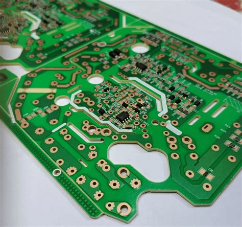
Modern PCB assembly processes have become the backbone of high-density electronics, driven by advancements in surface-mount technology (SMT). At the core of these innovations lies precision assembly, which ensures accurate placement of ultra-miniaturized components like 01005 resistors and micro-BGAs. Automated pick-and-place systems, combined with laser-aligned vision systems, achieve tolerances under 25µm, enabling seamless integration into compact designs.
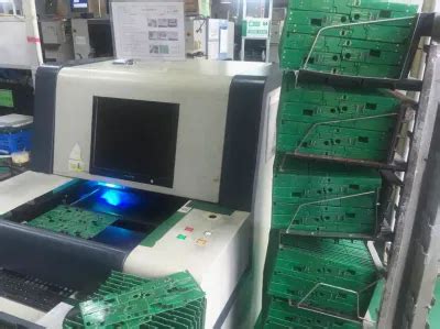
Equally critical are thermal management strategies that address heat dissipation challenges in PCBA layouts. Techniques such as embedded copper slugs and thermal vias mitigate hotspots, while advanced soldering methods like vacuum reflow reduce voiding in high-density interconnects. These processes are complemented by automated optical inspection (AOI) systems, which scan for defects at resolutions exceeding 20MP, ensuring reliability in mission-critical applications.
The shift toward heterogeneous integration further underscores the importance of PCB assembly in modern electronics. By combining system-in-package (SiP) designs with fine-pitch components, manufacturers achieve 30% higher component density compared to traditional methods. Rigorous environmental stress testing, including thermal cycling and vibration simulations, validates the durability of these assemblies under extreme conditions.
Looking ahead, innovations like laser-direct structuring (LDS) and adaptive stencil printing are set to redefine PCBA standards. These technologies enable real-time adjustments during production, reducing waste and improving yield rates for complex, high-layer-count boards. As the demand for IoT and wearable devices grows, these advancements position SMT as the cornerstone of next-generation electronics manufacturing.

Precision Assembly Techniques for SMT PCBs
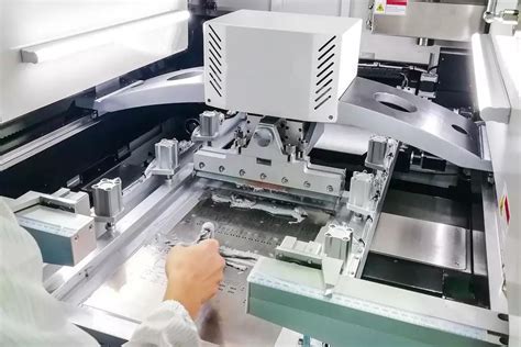
Modern PCB assembly relies on advanced precision techniques to address the complexities of high-density electronics. At the core of SMT (Surface Mount Technology) manufacturing lies the need for micron-level accuracy in component placement, solder paste application, and thermal profiling. Automated pick-and-place systems equipped with vision alignment capabilities now achieve placement tolerances below 20μm, enabling reliable mounting of ultra-fine-pitch components such as 01005 resistors and 0.3mm-pitch BGAs.
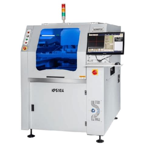
Tip: For high-yield PCBA production, maintain solder paste viscosity within 800–1,200 kcps to prevent bridging in densely packed layouts.
Innovations like laser-assisted soldering and 3D solder paste inspection (SPI) systems have elevated process control. These tools detect voids, insufficient deposits, or misalignments in real time, reducing rework rates by up to 40%. Additionally, nitrogen-reflow environments minimize oxidation during soldering, critical for preserving the integrity of microvias and thin copper traces.
Key advancements:
- Stencil design optimization: Laser-cut apertures with trapezoidal walls improve paste release for miniaturized pads.
- Dynamic thermal profiling: Adaptive oven zones compensate for board warpage, ensuring consistent joint formation across large panels.
- In-line AOI (Automated Optical Inspection): High-resolution cameras paired with machine learning algorithms identify tombstoning or skew defects at speeds exceeding 30 panels per hour.
The shift toward heterogeneous integration in PCB assembly demands tighter coordination between design and manufacturing teams. For instance, embedding 0201-sized passives beneath ICs requires precise solder jetting techniques to avoid shadowing effects. As PCBA processes evolve, balancing speed and precision remains pivotal for meeting the reliability standards of aerospace, medical, and 5G applications.
Miniaturization Strategies in SMT PCB Design
The relentless push toward smaller, more powerful electronic devices demands innovative approaches to PCB assembly, particularly in surface-mount technology (SMT) design. Achieving miniaturization without compromising functionality requires a strategic balance between component density, thermal performance, and signal integrity. Modern PCBA workflows now prioritize the use of ultra-compact components, such as 01005 packages (0.4 mm × 0.2 mm), alongside advanced substrate materials like polyimide-flex hybrids that enable thinner, lighter boards.
A critical enabler of miniaturization is embedded component technology, where passive elements like resistors and capacitors are integrated directly into the PCB substrate. This reduces surface-area consumption by up to 40% compared to traditional placement methods. Designers also leverage high-density interconnect (HDI) layouts with microvias (≤100 μm diameter) and staggered via-in-pad configurations to optimize routing in constrained spaces. For instance, stacked microvias allow vertical interconnections across multiple layers, freeing horizontal space for additional components.
However, shrinking form factors introduce challenges in PCB assembly reliability. Coefficient of thermal expansion (CTE) mismatches between materials become more pronounced, risking solder joint fractures during thermal cycling. To mitigate this, engineers employ adaptive soldering profiles and low-temperature solder alloys like Sn-Bi-Ag, which reduce thermal stress while maintaining joint strength. Additionally, laser-direct imaging (LDI) systems enhance alignment precision during PCBA, achieving placement accuracies of ±15 μm for components smaller than 1 mm².
Another emerging strategy involves 3D packaging techniques such as system-in-package (SiP) and chip-on-board (CoB) architectures. These methods consolidate multiple ICs into a single modular unit, drastically reducing the footprint while improving electrical performance. When combined with automated optical inspection (AOI) systems, these approaches ensure defect rates remain below 50 ppm even in high-density configurations.
As miniaturization continues to redefine SMT PCB manufacturing, designers must also address signal integrity through impedance-controlled routing and electromagnetic interference (EMI) shielding. Techniques like ground-plane partitioning and differential pair routing preserve signal clarity in tightly packed layouts, ensuring compliance with high-speed communication standards. By integrating these strategies, modern PCBA processes deliver compact, high-performance solutions that meet the demands of next-generation electronics.
Enhancing Reliability in High-Density SMT Assembly
Achieving reliability in high-density PCB assembly requires addressing challenges posed by shrinking component sizes and increasing thermal stresses. Modern surface-mount technology (SMT) processes leverage precision PCBA workflows to ensure robust interconnections, even with micro-BGA packages or 0201 passives. A critical factor lies in optimizing solder paste deposition through advanced stencil designs, such as laser-cut nano-coated apertures, which reduce voiding and improve joint integrity.
| Challenge | Solution | Impact |
|---|---|---|
| Thermal Cycling Stress | High-Tg FR-4 substrates | 25% longer lifespan under 150°C conditions |
| Microvoid Formation | Nitrogen-reflow environments | <2% void rate in 0.3mm pitch components |
| Signal Integrity Loss | Embedded passive materials | 40% reduction in crosstalk at 5GHz+ signals |
To further mitigate failure risks, manufacturers implement automated optical inspection (AOI) paired with 3D X-ray verification. These systems detect sub-5μm misalignments in PCB assembly lines, ensuring compliance with IPC-A-610 Class 3 standards. Additionally, underfill encapsulation protocols for CSPs (Chip Scale Packages) enhance mechanical stability, reducing solder joint fractures by up to 60% in vibration-prone environments.
Material selection plays an equally vital role. Low-loss laminates like Megtron 6 and halogen-free solder masks minimize signal attenuation while meeting RoHS directives. For mission-critical PCBA applications, accelerated life testing (ALT) simulates 10-year operational cycles in 72 hours, validating design choices against thermal expansion mismatches.
As component densities escalate, conformal coating techniques evolve to protect sub-100μm traces without impeding reworkability. Ultraviolet-curable acrylics now achieve 15μm-thick barriers with 500V/mil dielectric strength, balancing protection and repairability in compact IoT and automotive modules. By integrating these innovations, the industry sustains Moore’s Law for PCB assembly while maintaining field failure rates below 50ppm.
Advanced SMT Processes for Compact Electronics
The evolution of PCB assembly techniques has become pivotal in addressing the growing demand for compact, high-performance electronics. Modern SMT (Surface Mount Technology) processes now leverage ultra-precise component placement and microscopic soldering methods to accommodate shrinking device footprints without compromising functionality. For instance, automated optical inspection (AOI) systems paired with 3D solder paste inspection (SPI) ensure micron-level accuracy during PCBA stages, critical for aligning miniaturized components like 01005 resistors or micro BGAs.
A key advancement lies in the adoption of ultra-fine pitch components, enabling designers to achieve high-density interconnects (HDI) on multilayer boards. This is further enhanced by laser-direct imaging (LDI), which patterns solder masks with resolutions below 10µm, essential for avoiding bridging in tightly spaced layouts. Additionally, no-clean flux formulations and nitrogen-reflow environments are minimizing voiding risks in micro joints, directly boosting the reliability of PCB assembly in mission-critical applications.
Equally important is the integration of advanced materials into SMT workflows. Low-temperature solder alloys, such as SAC305 variants, reduce thermal stress on delicate components during PCBA, while high-Tg laminates provide dimensional stability for warpage-prone substrates. For ultra-compact designs, manufacturers are adopting embedded component technology, where passive elements are buried within the PCB layers—a process requiring precise control over lamination pressures and curing cycles.
Looking forward, the shift toward heterogeneous integration is redefining SMT PCB manufacturing. By combining chip-on-board (CoB) and system-in-package (SiP) approaches with traditional SMT, engineers achieve unprecedented functional density. This hybrid methodology relies on adaptive pick-and-place systems capable of handling components as thin as 0.2mm, paired with AI-driven process optimization to balance throughput and yield.
As these innovations mature, they enable PCBA specialists to overcome the "miniaturization paradox"—delivering more powerful electronics in smaller form factors while maintaining robust thermal and mechanical performance. The result is a new generation of devices where every square millimeter of board space is optimized through intelligent SMT process design.
Thermal Management Solutions for SMT PCBs
Effective thermal management in SMT PCB manufacturing is critical for maintaining the performance and longevity of high-density electronics. As components shrink and power densities rise in modern pcb assembly, managing heat dissipation becomes a pivotal challenge. Excessive heat not only degrades solder joint integrity but also accelerates component failure, particularly in densely packed pcba designs.
One innovative approach involves integrating thermal interface materials (TIMs) such as thermally conductive adhesives or phase-change compounds. These materials bridge gaps between heat-generating components and heatsinks, optimizing thermal transfer in high-density PCB assemblies. Advanced pcba designs also leverage embedded copper pours and thermal vias—microscopic channels that redirect heat away from sensitive areas—to enhance airflow and reduce localized hotspots.
For applications requiring active cooling, engineers are adopting micro-heat sinks and miniature fans directly mounted on SMT PCBs. These solutions complement passive strategies like strategic component placement, where high-power devices are positioned to maximize exposure to airflow. Notably, the use of low-thermal-resistance substrates—such as metal-core or ceramic-based laminates—has gained traction in power electronics, offering superior heat dissipation compared to traditional FR-4 materials.
Simulation tools play a vital role in preempting thermal issues. Finite element analysis (FEA) software models heat distribution across pcb assembly layouts, enabling designers to refine thermal vias and component spacing before prototyping. Post-production validation through infrared thermography ensures compliance with thermal thresholds, a key step in quality control for SMT manufacturing.
Emerging materials like graphene-enhanced thermal pads and liquid-cooled PCB layers represent the next frontier in thermal management. These innovations address the escalating demands of 5G infrastructure and AI-driven systems, where SMT PCB manufacturing must balance miniaturization with uncompromised thermal stability. By integrating these strategies, manufacturers achieve reliable operation in extreme environments while extending the lifecycle of advanced electronics.
Quality Control in SMT PCB Manufacturing
Effective quality control is the cornerstone of reliable PCB assembly processes, particularly for high-density electronics requiring micron-level precision. Modern PCBA workflows integrate automated optical inspection (AOI) systems that leverage machine vision algorithms to detect solder joint defects, component misalignments, and substrate imperfections at speeds exceeding 10,000 inspections per hour. These systems complement X-ray fluorescence (XRF) testing, which verifies solder alloy composition and thickness to ensure compliance with IPC-A-610 standards for aerospace and medical-grade assemblies.
Advanced manufacturers employ statistical process control (SPC) methodologies, correlating real-time data from pick-and-place machines and reflow ovens to predict potential SMT PCB failures. This proactive approach reduces defect rates by 35–50% compared to traditional post-production sampling. For mission-critical applications, environmental stress screening (ESS) subjects boards to accelerated thermal cycling and vibration tests, simulating decades of operational wear in controlled chambers.
The shift toward 0201 metric components and 0.3mm-pitch BGAs has necessitated 3D solder paste inspection (SPI) systems that map deposition volumes with ±5μm accuracy. Combined with impedance testing for high-frequency circuits, these tools address signal integrity challenges in 5G and IoT devices. Leading PCB assembly providers now implement blockchain-enabled traceability systems, creating immutable records of material sourcing, process parameters, and test results for each PCBA unit—a critical feature for automotive ISO/TS 16949 certifications.
By synchronizing these layered inspection protocols with AI-driven analytics, manufacturers achieve first-pass yield (FPY) rates exceeding 99.2% even for complex HDI designs, while reducing corrective action timelines by 60%. This multilayered QC framework ensures that SMT PCB manufacturing delivers the reliability demanded by next-generation compact electronics without compromising throughput scalability.
Future Trends in SMT Technology for Electronics
The evolution of SMT PCB manufacturing is accelerating to meet the demands of next-generation electronics, driven by advancements in miniaturization, automation, and material science. As devices shrink and performance expectations rise, manufacturers are adopting pcb assembly techniques that integrate artificial intelligence for real-time defect detection. Machine learning algorithms now optimize pick-and-place accuracy to handle components as small as 01005 packages, enabling pcba workflows to achieve unprecedented precision in high-density layouts.
Emerging heterogeneous integration methods are redefining SMT PCB manufacturing by combining traditional surface-mount processes with chip-on-board (CoB) and system-in-package (SiP) architectures. This hybrid approach reduces signal loss in millimeter-wave applications, critical for 5G and IoT devices. Meanwhile, advancements in conductive adhesives and low-temperature solders are addressing thermal stress challenges in pcb assembly, particularly for flexible and stretchable substrates used in wearable electronics.
The shift toward sustainable manufacturing is also reshaping pcba practices. Novel halogen-free solder masks and recyclable substrates are gaining traction, aligning with global circular economy initiatives. Additionally, inline 3D SPI (Solder Paste Inspection) systems paired with AOI (Automated Optical Inspection) are reducing material waste by 22% in SMT PCB manufacturing lines.
Looking ahead, quantum computing-ready designs will push SMT PCB manufacturing toward ultra-high-frequency capabilities, requiring substrates with dielectric constants below 2.5. The integration of photonic components into pcb assembly workflows is another frontier, with laser-assisted placement systems enabling precise alignment of optical interconnects. These innovations, coupled with blockchain-based traceability systems, will ensure pcba processes meet both performance benchmarks and stringent supply chain transparency requirements.

High-Density PCB Design with SMT Innovations
Modern PCB assembly demands innovative approaches to accommodate the escalating complexity of high-density electronics. Leveraging SMT (Surface Mount Technology) advancements, designers now achieve unprecedented component density without compromising performance. A critical innovation lies in precision placement systems, which enable the accurate positioning of ultra-miniaturized components such as 01005 resistors and micro-BGA packages. These systems, combined with advanced solder paste formulations, ensure reliable electrical connections even at sub-0.4mm pitch spacings.
To optimize space utilization, designers employ 3D stacking techniques and embedded passive components within multilayer PCBA (Printed Circuit Board Assembly) designs. This approach reduces footprint while enhancing signal integrity—a necessity for applications like IoT devices and wearable tech. Additionally, laser-direct imaging (LDI) and hybrid solder mask technologies improve trace resolution, supporting finer line widths (down to 25µm) and tighter tolerances.
Thermal management remains a pivotal challenge in high-density layouts. Innovations such as thermal via arrays and embedded copper coins efficiently dissipate heat from power-hungry components like FPGAs and processors. Pairing these with low-thermal-resistance substrates ensures stable operation in demanding environments.
For reliability, automated optical inspection (AOI) systems integrated into PCB assembly lines detect micro-defects, such as tombstoning or insufficient solder, at early stages. Advanced conformal coatings and underfill materials further protect against mechanical stress and environmental factors.
The synergy between SMT innovations and high-density design principles continues to redefine what’s possible in electronics miniaturization, enabling smarter, faster, and more compact devices without sacrificing durability or functionality.
Conclusion
The evolution of SMT PCB manufacturing has redefined the boundaries of modern electronics, particularly in enabling high-density designs that demand unparalleled precision and reliability. As industries push toward smaller, faster, and more complex devices, the integration of advanced PCB assembly (PCBA) techniques has become indispensable. Innovations such as laser-direct imaging for ultra-fine traces and automated optical inspection (AOI) systems ensure that miniaturized components are placed with micrometer-level accuracy, directly addressing the challenges of thermal management and signal integrity in compact layouts.
A critical factor in this progress lies in the synergy between precision assembly workflows and robust material science. High-performance substrates, coupled with low-temperature soldering alloys, mitigate warping risks while maintaining electrical stability—a necessity for high-density PCB assembly. Furthermore, the adoption of 3D printing for custom jigs and fixtures streamlines prototyping, reducing time-to-market for cutting-edge applications like wearable tech and IoT modules.
Quality assurance remains paramount, with PCBA providers leveraging AI-driven defect detection and real-time process monitoring to achieve near-zero ppm defect rates. These advancements not only enhance reliability but also extend the lifecycle of electronics operating in harsh environments. Looking ahead, the convergence of SMT innovations with emerging technologies such as embedded components and additive manufacturing will continue to drive the industry toward thinner, lighter, and more power-efficient solutions. By prioritizing scalability and sustainability, manufacturers are poised to meet the escalating demands of 5G, AI-driven systems, and next-generation consumer electronics.
FAQs
What distinguishes PCB assembly from PCBA in modern manufacturing?
PCB assembly refers to the process of populating a bare circuit board with electronic components, while PCBA (Printed Circuit Board Assembly) denotes the completed board with all components soldered and tested. The distinction lies in functional readiness—PCBA implies a fully operational unit ready for integration into end devices.
How do miniaturization strategies impact high-density SMT PCB reliability?
Advanced laser-direct imaging and microvia drilling enable precise placement of 01005 passives and 0.3mm pitch BGAs. However, thermal stress management becomes critical. Manufacturers counter this with low-solder-voiding pastes and automated optical inspection (AOI) systems to maintain ≥99.9% post-reflow yield rates.
Can thermal management solutions coexist with high-density PCB design?
Yes. Techniques like embedded copper substrates and thermal vias are integrated during PCB assembly to dissipate heat without compromising layout density. For PCBA in 5G modules, 3D-printed heat sinks are often co-designed with RF circuitry to balance signal integrity and thermal performance.
What quality control methods ensure SMT PCB manufacturing consistency?
Inline SPI (Solder Paste Inspection) and X-ray tomography are deployed at PCBA stages to detect micro-cracks and head-in-pillow defects. Statistical process control (SPC) tools track CpK values >1.67 for critical parameters like reflow oven temperature profiles.
Are automated optical inspection (AOI) systems sufficient for high-density electronics?
While AOI handles ≥98% of visible defects, cross-sectional analysis and ion chromatography are increasingly paired with AOI to validate solder joint alloys and ionic contamination levels below 1.56 μg/cm² for aerospace-grade PCB assembly.
Explore Advanced SMT Solutions Today
For tailored PCB assembly workflows optimized for high-density applications, please click here to consult our PCBA engineering team about zero-defect manufacturing protocols and IoT-optimized SMT lines.