How to achieve perfect PCB welding
In the manufacturing process of modern electronic products, PCB (printed circuit board) welding is a crucial link. The quality of welding directly affects the performance, reliability and life of electronic products. Therefore, it is very necessary for electronic engineers and technicians to master the skills and precautions of welding. This article will elaborate on how to achieve perfect PCB welding from multiple aspects such as preparation before welding, skills during welding, inspection and maintenance after welding.
1.Preparation before welding
(1)Choose the right material
Before PCB welding, you must first choose the right welding material, including solder, flux and welding tools.
Solder: Commonly used solders are lead-tin alloy and lead-free tin alloy. Lead-tin alloy solder has good fluidity during welding, but due to the toxicity of lead, many countries and regions have gradually banned it. Although lead-free solder is environmentally friendly, its welding temperature is higher and its fluidity is slightly worse, so it needs to be selected according to the specific situation.
Flux: Flux can improve the fluidity of solder, reduce the generation of oxides, and ensure the quality of welding. Choosing the right flux is crucial for the welding effect.
(2)Prepare tools
The selection and preparation of welding tools are also the key to successful welding. Commonly used welding tools include:
Soldering iron: Choose a suitable soldering iron, the power is generally between 30W-60W, and the temperature-adjustable soldering iron is more ideal.
Soldering table: A stable soldering table can improve work efficiency and avoid welding defects caused by improper operation.
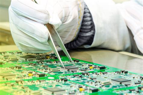
Tweezers and scissors: used to clamp components and trim excess pins.
Cleaning tools: such as cleaning cloth, alcohol, etc., used to clean the PCB surface and welding tools.

(3)Preparation of PCB
Before welding, the PCB needs to be thoroughly inspected and cleaned:
Check the PCB: Make sure that the PCB is not damaged, the pads are intact, and the lines are clear.
Clean the surface: Use detergent and non-woven cloth to clean the PCB surface, remove oil and dust to ensure the welding effect.
2.Skills in the welding process
(1)Temperature control
Temperature control is crucial during welding. The temperature of the soldering iron should be adjusted according to the type of solder used:
Lead-tin alloy: generally around 350℃.
Lead-free solder: The temperature should be around 370℃.
Too high a temperature can cause damage to the PCB and components, while too low a temperature can cause poor soldering.
(2)Soldering skills
Soldering order: Generally, soldering is performed from small components to large components, from the center to the edge. This can avoid the movement of small components due to the soldering of large components.
Soldering time: The soldering time of each solder joint should be controlled within 2-3 seconds to avoid damage to components caused by heating for too long.
Soldering angle: The angle between the soldering iron and the PCB should be kept at about 45 degrees to facilitate the flow and infiltration of solder.
Formation of solder joints: When soldering, first place the soldering iron on the pad and component pins, and then add solder after it is heated to ensure that the solder flows evenly and forms a good solder joint.
(3)Use of flux
The use of flux can significantly improve the quality of soldering. Attention should be paid when using:
Appropriate use: The flux should not be excessive to avoid leaving residues after soldering.
Clean residue: After welding, the PCB surface should be cleaned in time to remove the flux residue to avoid affecting the circuit.

3.Inspection and maintenance after welding
(1)Solder joint inspection
After welding, the solder joints need to be carefully inspected. Qualified solder joints should have the following characteristics:
Smooth and flat: The solder joints should be smooth and have no obvious solder balls or cold soldering.
Regular shape: The solder joints should be round or slightly flat and tightly combined with the pads.
No short circuit: Check whether there is a short circuit between the solder joints. If necessary, use a multimeter to test.
(2)Functional test
After welding, functional testing is a key step to ensure the normal operation of the PCB. Testing can be performed in the following ways:
Power-on test: Observe whether the circuit is working properly after power-on and check whether there is abnormal heating of components.
Signal test: Use tools such as oscilloscopes to check whether the signal waveform is normal.

(3)Maintenance and care
In order to ensure the long-term stability of PCB, maintenance and care after welding are equally important:
Regular inspection: Check the PCB regularly and deal with problems in time.
Moisture and dustproof: Keep the PCB dry and clean to prevent moisture and dust from affecting the circuit.
Proper storage: When not in use, the PCB should be properly stored to avoid mechanical damage and electrostatic damage.
4. Summary
Perfect PCB welding requires not only solid theoretical knowledge, but also rich practical experience. By reasonably selecting materials, mastering welding skills, strictly controlling temperature, and meticulous inspection and maintenance, the welding quality can be significantly improved to ensure the performance and reliability of electronic products. It is hoped that the welding methods and techniques described in this article can provide help to the majority of electronic engineers and technicians, and help them achieve greater success in the field of PCB welding.
