Hidden dangers of advanced design in PCB design
PCB circuit designers need to implement the required functions in PCB circuit design according to the circuit schematic. PCB circuit design is a very complex and technical job. Usually, beginners of PCB circuit design will encounter many problems.
This article lists the technical specifications and some advanced design errors in PCB circuit design.
It is hoped that PCB circuit designers can continuously improve in circuit design through continuous learning and experience accumulation, achieve excellent circuit performance and heat dissipation performance, and effectively save production costs.
PCB technical specification content:
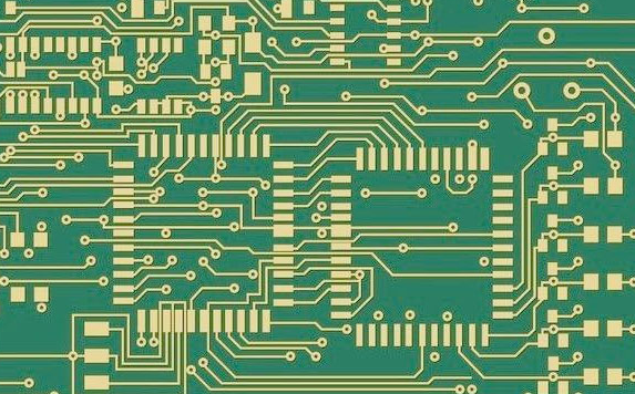
1.PCB wiring and layout
PCB wiring and layout isolation criteria: strong and weak current isolation, large and small voltage isolation, high and low frequency isolation, input and output isolation, digital analog isolation, input and output isolation, the boundary standard is one order of magnitude difference. Isolation methods include: space away and ground wire separation.
Let the analog and digital circuits have their own power supply and ground path respectively. If possible, the power supply and ground of these two parts of the circuit should be widened as much as possible or separate power supply layers and ground layers should be used to reduce the impedance of the power supply and ground loop and reduce any interference voltage that may be in the power supply and ground loop.
When designing a multilayer printed circuit board, separate the digital circuit and the analog circuit. If conditions permit, arrange the digital circuit and the analog circuit in different layers. If they must be arranged on the same layer, you can use trenching, adding grounding lines, separation and other methods to remedy it. The analog and digital ground and power supplies must be separated and cannot be mixed.
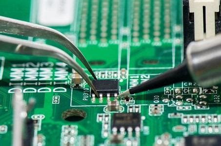
2.Circuit design
Signal filter leg coupling: For each analog amplifier power supply, a decoupling capacitor must be added between the connection closest to the circuit and the amplifier. For digital integrated circuits, decoupling capacitors are added in groups. Install capacitor bypass on the brushes of the motor and generator, connect R-C filters in series on each winding branch, and add low-pass filtering at the power supply inlet to suppress interference. The filter should be installed as close as possible to the device to be filtered, and a short, shielded lead should be used as a coupling medium. All filters must be shielded, and the input leads should be isolated from the output leads.
Signal termination: Impedance matching between the source and the destination of a high-frequency circuit is very important. Wrong matching will cause signal feedback and damped oscillation. Excessive RF energy will cause EMI problems. At this time, it is necessary to consider using signal termination. There are several types of signal termination: series/source termination, parallel termination, RC termination, Thevenin termination, and diode termination.
3.Housing
The shield has the least number of seams; at the seams of the shield, the multi-point spring pressure contact method has good electrical continuity; the ventilation hole D<3mm, this aperture can effectively prevent large electromagnetic leakage or entry;
The shield opening (such as the ventilation hole) is blocked with a fine copper mesh or other appropriate conductive materials; if the metal mesh of the ventilation hole needs to be removed frequently, it can be fixed around the hole with screws or bolts, but the screw spacing is <25mm to maintain continuous line contact.
4.Device selection
Capacitors should try to choose chip capacitors with small lead inductance. For the bypass capacitor of the stable power supply, choose electrolytic capacitors, and for the capacitors for AC coupling and charge storage, choose polytetrafluoroethylene capacitors or other polyester capacitors (polypropylene, polystyrene, etc.).
The standard for capacitor selection is: the lowest possible ESR capacitor; the highest possible resonant frequency value of the capacitor.
When selecting a filter connector, in addition to the factors to be considered when selecting an ordinary connector, the cutoff frequency of the filter should also be considered. When the signal frequencies transmitted on each core wire in the connector are different, the cutoff frequency should be determined based on the signal with the highest frequency.
In addition to the above PCB design specifications, there are some problems that are often caused by the carelessness of PCB engineers.
The following are some common advanced mines for PCB circuit workers:
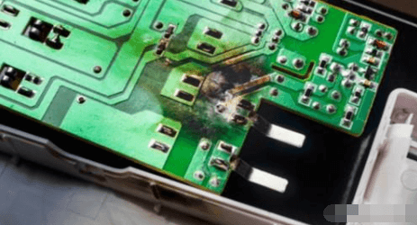
- When making a four-side pin package according to the device specification, the distance between the two side pins is too close, but because the specification is like this, the hand slips and ignores it, and it may be short-circuited in the later processing.
- During the design stage, run DRC to check the safety spacing. In addition, are there any irrelevant lines involved in the opening of the solder mask layer? If so, a short circuit with the shield cover ground can be caused after soldering the shield cover.
- During the design stage, run DRC to check the safety spacing. In addition, are there any irrelevant lines involved in the opening of the solder mask layer? If so, a short circuit with the shield cover ground can be caused after soldering the shield cover.
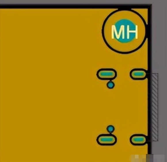
- The network with electrical properties is too close to the screw hole. After multiple board installations and disassemblies, the green (lan) oil may be worn off, which may easily cause a short circuit to the screw. In order to prevent this potential hidden danger, draw a prohibited area on the screw hole and avoid the distance during design.
- When outputting files, whether there are 2D lines and texts on the electrical layer, causing the 2D lines and texts on the CAM file to become “networks” with electrical properties
- When designing a board, a handle should be made on the edge of the chassis, and the ground inside the board is prohibited from being poured into the edge of the board (the specific amount depends on the actual situation). After multiple frictions and the green (lan) oil is worn off, it is easy to cause a short circuit between the board and the chassis ground.
So is there a way to avoid and check such design problems and mines in the design stage?
Here I share a self-used PCB manufacturability design analysis software: Huaqiu DFM. This software can support one-click import of PCB design files for design analysis in the design stage, check whether the PCB design specifications meet the DFM requirements, accurately locate design risks, and support one-click output of gerber (Altium Designer, Protel, PADS, Allegro are no problem), bom, coordinate files, etc.