How to design RF and analog circuits on the same PCB?
The popularity of handheld wireless communication devices and remote control devices has driven a significant increase in the demand for mixed analog, digital and RF design. Handheld devices, base stations, remote controls, Bluetooth devices, computer wireless communication functions, many consumer electronics, and military/aerospace systems now require RF technology.
For many years, RF design has required professional designers using specialized design and analysis tools. Typically, the RF portion of the PCB is designed by RF professionals in a separate environment and then merged with the rest of the mixed technology PCB. This process is inefficient and often requires repeated design and multiple unrelated databases to integrate with mixed technologies.
In the past, design functions were performed and repeated in two design environments and connected by a non-intelligent ASCII interface (Figure 1 (a)). The PCB system design and RF-specific design systems in the two environments have their own libraries, RF design databases, and design archives. This requires that the design data (schematics and layouts) and libraries in the two environments be managed and synchronized through a cumbersome ASCII interface.
In this old approach, RF designers develop RF circuits in isolation from the rest of the PCB system design. The RF circuits are then translated into the overall PCB design using ASCII files to create schematics and physical implementations on the main PCB. If there are problems with the RF circuits, the design must be corrected in the separate RF solution and then translated back into the main PCB.
The RF simulator simulates only ideal RF circuits.
In real mixed system implementations, there are many fragmented ground planes, ground planes, and adjacent RF circuits, which makes analysis very difficult, and everyone knows that these additional shapes will have a lasting impact on the operation of the RF circuits.
This old approach has been successfully used for mixed-signal board design for many years, but as the RF content of products has increased, the problems caused by two independent design systems have begun to affect designer productivity, time to market, and product quality.
To address these issues, Mentor Graphics has developed a dynamic linking technology that integrates PCB schematic and layout tools with RF design and simulation tools, resulting in a new solution that overcomes the shortcomings of traditional RF design.

RF Aware PCB Design
To maintain design intent between PCB and RF design, RF design tools must understand the layer-oriented structure of the PCB layout, and the PCB system must understand the parameterized planar microwave components used in the RF design environment.
Another key issue is that the PCB system structures the layout of the RF circuit as a short circuit, which prevents the design from being properly designed and checked (DRC). For today’s complex RF system designs, functional RF-aware DRC is a must for the design methodology to ensure the design is correct.
All of this helps maintain design intent
Maintaining design intent is critical because it is the basis for enabling multiple round trips of design data between tool sets without losing information.
RF design is an iterative process that requires many steps to adjust and optimize the design. In the past, it was very difficult to perform RF design in the context of a real PCB design. When an optimized RF module is implemented on the PCB, there is still no guarantee that it will still work optimally. As a verification, electromagnetic field analysis (EM) of the PCB implementation is required.
There are several problems with this design process.
First, the circuits were simulated as simple metal layer geometries, so the RF tools could not modify the metal layers and pass optimized results back to the PCB design and still have a good RF circuit. Second, the EM solution was time consuming.
In the new flow, because the PCB tools and RF tools share the design intent, the circuit can be passed between the tool sets without losing the design intent. This means that circuit simulation (very fast) and EM analysis (when needed) can be repeated, and the results can be compared for each circuit modification. All this is done in the real PCB environment, including ground planes, RF circuit layout, wires, vias and other components.
RF PCB Design Bottlenecks
The RF PCB design bottlenecks are mainly the following. First, because each RF module on the PCB board may have been designed by an independent RF design team, and each module can be independently upgraded, evolved and reused, it becomes critical to manage the entire circuit as a whole, but still access these modules as individual circuit elements at any time. To solve this problem, schematic and layout tools must be extended to support hierarchical grouping of circuits. With this approach, even if an RF circuit is already laid out on the PCB, it can still be placed as an RF circuit with other modules and can be connected to the appropriate RF design team for analysis.
The next obstacle is how to design the ground plane. In the traditional design process, RF metal is used as a black box metal block, and the spacing with the ground is done manually because the clearance must pass through each ground layer. When the RF circuit is updated (a frequent operation), the cut-out parts must be manually modified to correspond to the new circuit. For some designs, this editing process alone can take weeks.
New synthesis design flow
Synthesis between RF design tools and PCB design tools has always been based on the bidirectional conversion of ASCII IFF format files. Although this format can handle some design data, it is far from achieving seamless iterative synthesis. The lack of library synchronization is a fatal reason.
This design requirement has spawned a network-based tool communication that provides a dynamic bidirectional link between RF design and system-level PCB design (Figure 1 (b)). To support concurrent engineering processing, multiple PCB engineers can use the same design database at the same time, and each can link one or more analog parts. Now, RF modules can be designed using RF design tools and integrated as part of system-level schematics and PCBs when appropriate, rather than just an elusive black box circuit as in the past. At this stage, the circuit can be upgraded and its effects simulated in either environment.
Treat each RF circuit as a set of objects to help maintain traceability, version management, and design issues. Because the design intent is preserved, any number of design iterations can be implemented without time cost. In addition, because RF modules can be simulated in a real system-level PCB environment, their functions should be verified in more detail to help shorten the design cycle.
Minimize RF effects in PCB interconnection design
The interconnection of the circuit board system includes three types of interconnection: chip to circuit board, interconnection within the PCB board, and between the PCB and external devices. In RF design, the electromagnetic characteristics at the interconnection point are one of the main problems faced by engineering design. This article introduces various techniques for the above three types of interconnection design, including device mounting methods, wiring isolation, and measures to reduce lead inductance.
There are signs that the frequency of printed circuit board design is getting higher and higher. As data rates continue to increase, the bandwidth required for data transmission has also pushed the upper limit of signal frequency to 1GHz or even higher. Although this high-frequency signal technology is far beyond the range of millimeter wave technology (30GHz), it does involve RF and low-end microwave technology.
RF engineering design methods must be able to deal with the effects of stronger electromagnetic fields that are usually generated at higher frequencies. These electromagnetic fields can induce signals on adjacent signal lines or PCB lines, causing annoying crosstalk (interference and overall noise) and impairing system performance. Return loss is mainly caused by impedance mismatch and affects the signal in the same way as additive noise and interference.
High return loss has two negative effects: 1. Signals reflected back to the signal source increase system noise, making it more difficult for the receiver to distinguish between noise and signal; 2. Any reflected signal will basically degrade the signal quality because the shape of the input signal has changed.
Although digital systems only deal with 1 and 0 signals and have very good fault tolerance, the harmonics generated when high-speed pulses rise will cause the signal to become weaker at higher frequencies. Although forward error correction technology can eliminate some negative effects, part of the system’s bandwidth is used to transmit redundant data, resulting in reduced system performance. A better solution is to make RF effects contribute to rather than harm signal integrity. It is recommended that the total return loss at the highest frequency of the digital system (usually the worst data point) is -25dB, equivalent to a VSWR of 1.1.
The goal of PCB design is smaller, faster and less expensive. For RFPCB, high-speed signals sometimes limit the miniaturization of PCB design. At present, the main method to solve the crosstalk problem is to manage the ground layer, space between the wiring and reduce the lead inductance (studcapacitance). The main method to reduce return loss is impedance matching. This method includes effective management of insulating materials and isolation of active signal lines and ground lines, especially spacing between signal lines and ground where the state jumps.
Since the interconnection point is the weakest link in the circuit chain, in RF design, the electromagnetic properties at the interconnection point are the main problems faced by engineering design. Each interconnection point should be examined and the existing problems should be solved. The interconnection of the circuit board system includes three types of interconnection: chip to circuit board, interconnection within the PCB board, and signal input/output between the PCB and external devices.
- Interconnection between chip and PCB board
Pentium IV and high-speed chips with a large number of input/output interconnection points have been launched. As far as the chip itself is concerned, its performance is reliable and the processing speed has reached 1GHz. At the recent GHz Interconnection Seminar (www.az.ww.com), the most exciting thing was that the methods for dealing with the problem of growing I/O numbers and frequencies have been widely known. The main problem with the interconnection between chips and PCBs is that the interconnection density is too high, which will cause the basic structure of the PCB material to become a factor limiting the growth of interconnection density. An innovative solution proposed at the meeting is to use a local wireless transmitter inside the chip to transmit data to a nearby circuit board.
Whether this solution works or not, the participants are very clear: IC design technology is far ahead of PCB design technology in terms of high-frequency applications.
- Interconnection within PCB board
The skills and methods for high-frequency PCB design are as follows:
- The corner of the transmission line should be 45° to reduce return loss (Figure 1);
- Use high-performance insulating circuit boards with strictly controlled insulation constant values according to the level. This method is conducive to the effective management of the electromagnetic field between the insulating material and the adjacent wiring.
- Improve the PCB design specifications for high-precision etching. Consider the total error of the line width of +/-0.0007 inches, manage the undercut and cross-section of the wiring shape, and specify the plating conditions of the wiring sidewall. Overall management of the wiring (conductor) geometry and coating surface is very important to solve the skin effect problems related to microwave frequencies and achieve these specifications.
- If there is a tap inductance on the protruding lead, avoid using components with leads. In high-frequency environments, it is best to use surface-mount components.
- For signal vias, avoid using the through hole processing (PTH) process on sensitive boards because it will cause lead inductance at the via. For example, when a via on a 20-layer board is used to connect layers 1 to 3, the lead inductance can affect layers 4 to 19.
- Provide abundant ground planes. Use molded holes to connect these ground planes to prevent the influence of 3D electromagnetic fields on the circuit board.
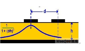
- Choose electroless nickel plating or immersion gold plating instead of HASL plating. This electroplated surface can provide better skin effect for high-frequency current (Figure 2). In addition, this highly solderable coating requires fewer leads, which helps reduce environmental pollution.
- The solder mask prevents the flow of solder paste. However, due to the uncertainty of thickness and the unknown insulation performance, covering the entire board surface with solder mask will lead to large changes in electromagnetic energy in microstrip design. Solder dam is generally used as solder mask.
If you are not familiar with these methods, you can consult experienced design engineers who have worked on military microwave circuit boards. You can also discuss with them the price range you can afford. For example, using a copper-backed coplanar microstrip design is more economical than a stripline design. You can discuss this with them to get better advice. Good engineers may not be used to considering cost issues, but their advice is also very helpful. Now we should try to train young engineers who are unfamiliar with RF effects and lack experience in dealing with RF effects. This will be a long-term task.
In addition, other solutions can be adopted, such as improving computer models to enable them to have RF effect processing capabilities.
Three, PCB and external device interconnection
Now we can think that we have solved all signal management problems on the board and the interconnection of each discrete component. So how to solve the signal input/output problem from the circuit board to the wire connecting the remote device? Trompeter Electronics, an innovator in coaxial cable technology, is working on this problem and has made some important progress (Figure 3). In addition, look at the electromagnetic field given in Figure 4. In this case, we are managing the transition from microstrip to coax. In coax, the ground planes are woven in a ring and spaced evenly. In microstrip, the ground plane is underneath the active lines. This introduces certain edge effects that need to be understood, predicted, and accounted for during design. Of course, this mismatch also results in return loss, which must be minimized to avoid noise and signal interference.
Managing impedance issues within the board is not a design issue that can be ignored. Impedance starts at the surface of the board, then passes through a solder joint to the connector and ends at the coax. Since impedance varies with frequency, the higher the frequency, the more difficult it is to manage impedance. The problem of transmitting signals at higher frequencies over a wide bandwidth seems to be a major issue faced in the design.