9 Factors That Lead to Signal Integrity Issues in PCBs
Avoiding signal integrity issues in PCBs is an extremely complex task for designers. It requires an understanding of signal integrity design rules and techniques. With the introduction of faster logic families, designers have realized that simple PCB layouts cannot meet the requirements of signal integrity.
High-speed designs come with special signal integrity issues that can give you headaches if not handled properly. Engineers are always advised to consider some of the best PCB design services to minimize signal integrity issues in the early design cycle, thereby avoiding costly design iterations.
As we continue, we will provide more insights on the following topics:
What is Signal Integrity in PCBs?
The Need for Signal Integrity in PCBs
9 Factors That Lead to Signal Integrity Issues in PCBs
What is Signal Integrity in PCBs?
Signal Integrity (SI) refers to the ability of a signal to propagate without distortion. Signal integrity is simply the quality of a signal passing through a transmission line. It gives a measurement of the amount of signal attenuation as the signal is transmitted from the driver to the receiver. This issue is not a major concern at lower frequencies, but it is an important factor to consider when PCBs operate at higher speeds and high frequencies (>50MHz). In the high frequency region, both digital and analog aspects of the signal need to be considered.
The Effect of Transmission Media on Signal Integrity.
When a signal propagates from a driver to a receiver, it does not remain unchanged and whatever was originally sent will be received with varying degrees of distortion. This signal distortion is caused by impedance mismatch, reflections, ringing, crosstalk, jitter and ground bounce. The designer’s first goal should be to minimize these factors so that the original signal reaches its destination with minimal distortion. In addition, special attention needs to be paid to maintain signal quality and control its undesirable effects in electronic circuits. Read our post on Controlled Impedance Routing with Altium .
The Need for Signal Integrity in PCBs
When we have signal integrity issues in PCBs, it may not work as expected. It may work in an unreliable way – sometimes it works and sometimes it doesn’t. It may work in the prototype stage but often fails in mass production; it may work in the lab but not reliably in the field; it works in old production batches but fails in new production batches, and so on. A signal is said to have lost integrity when:
It is deformed, that is, its shape changes from the desired shape
Unwanted electrical noise is superimposed on the signal, making it have a lower signal-to-noise ratio
It generates unnecessary noise for other signals and circuits on the board
A PCB is said to have the necessary signal integrity when:
All signals within it can propagate without distortion
Its devices and interconnections are not susceptible to extraneous electrical noise and electromagnetic interference (EMI) from other nearby electrical products and meet or exceed regulatory standards
It does not generate, introduce or radiate EMI in other circuits/cables/products associated with it or nearby that meet or exceed regulatory standards
9 Factors that cause signal integrity problems in PCBs
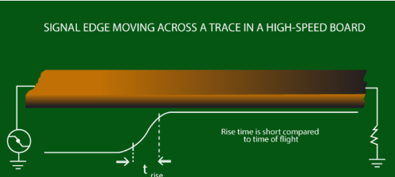
Perhaps the most important cause of signal integrity problems in PCBs is faster signal rise times. When circuits and devices operate at low to medium frequencies, signal integrity problems due to PCB design are rarely a problem. However, when we operate at high (RF and higher) frequencies, signal rise times are shorter and signal integrity due to PCB design becomes a very big problem.

Reducing rise time is critical to signal integrity.
Factors that cause signal integrity degradation in PCBs:
Generally speaking, fast signal rise times and high signal frequencies increase signal integrity issues. For analysis purposes, we can classify various signal integrity issues into the following categories:
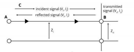
- Signal degradation due to uncontrolled line impedance
The quality of the signal on the network depends on the characteristics of the signal trace and its return path. When running on the line, if the signal encounters changes or unevenness in the line impedance, it will suffer reflections, resulting in ringing and signal distortion.
In addition, the faster the signal rise time, the greater the signal distortion caused by uncontrolled line impedance changes. We can minimize the signal distortion caused by reflections by reducing or eliminating changes in line impedance:
Ensure that the signal line and its return path act as uniform transmission lines with uniform controlled impedance.
With the signal return path, place it as a uniform plane close to the signal layer.
Ensure that the controlled impedance signal line sees matched source and receiver impedances – the same as the characteristic impedance of the signal line. This may require adding appropriate termination resistors at the source and receiver ends.
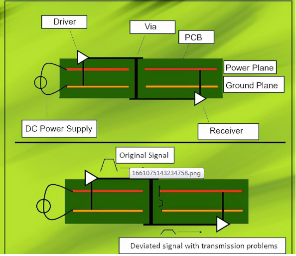
- Signal attenuation caused by other impedance discontinuities
image.png
Impedance discontinuities can cause ringing and signal distortion.
As mentioned earlier, if a signal encounters impedance discontinuities during transmission, it will suffer reflections, which can cause ringing and signal distortion. Discontinuities in line impedance occur when one of the following situations is encountered:
When a signal encounters a via in its path.
When a signal branches into two or more lines.
When a signal return path plane encounters a discontinuity, such as when a line stub is connected to a signal line, and a split occurs in the plane.
When a line stub is connected to a signal line.
When a signal line starts at the source end.
When a signal line terminates at the receiving end.
When a signal and loop are connected to a connector pin.
Moreover, the faster the signal rise time, the greater the signal distortion caused by impedance discontinuities.
We can sign off on discontinuities due to line impedance discontinuities:
Minimize the impact of discontinuities caused by vias and via stubs by using smaller microvias and HDI-PCB technology.
Reduce trace stub length
When a signal is used in multiple places, route the trace in a daisy-chain fashion rather than a multi-drop fashion.
Proper termination resistors at both the source and sink ends.
Use differential signals and tightly coupled differential pairs, which are inherently more immune to discontinuities in the signal return path plane.
Ensure that the signal lines are as short as possible and the signal return path is as wide as possible at the connector where the discontinuity occurs.
3.Signal attenuation caused by propagation delay
The transmission time of a signal from source to receiver on a PCB is finite. The signal delay is proportional to the length of the signal line and inversely proportional to the signal speed on a specific PCB layer. If the data signal and the clock signal do not match the overall delay, they will arrive at the receiver at different times for detection, which will cause signal distortion; excessive deviation will cause signal sampling errors. As the signal speed increases, the sampling rate is also higher and the allowed deviation is also smaller, resulting in a greater tendency for deviation.
Tip: The skew in a group of signal lines can be minimized by signal delay matching (mainly trace length matching).
4.Signal degradation due to signal attenuation
When a signal propagates on a PCB line, it is attenuated due to the conductive trace resistance (which increases at higher frequencies due to the skin effect) and the dielectric material loss factor Df. Both of these losses increase with increasing frequency, so the high-frequency components of the signal will experience greater attenuation than the low-frequency components; this results in a reduction in signal bandwidth, which then causes signal distortion due to increased signal rise time; excessive signal rise time can cause data detection errors.
Tip: When signal attenuation is an important consideration, it is important to select appropriate low-loss high-speed materials and properly control the geometry of the traces to minimize signal loss.
5.Signal degradation due to crosstalk noise
Crosstalk of adjacent PCB signal lines.
Rapid voltage or current transitions on a signal line or return path plane can couple to adjacent signal lines, generating unwanted signals called crosstalk and switching noise on adjacent signal lines. This coupling is due to mutual capacitance and mutual inductance between traces. This mutual coupling of capacitance and inductance can be reduced by increasing the space between traces. As a rule of thumb, the space should be three times the trace width (3W). As usual, faster rise time signals will generate more crosstalk and switching noise.
Crosstalk and switching noise can be reduced by:
Increase the spacing between adjacent signal traces.
Make the signal return path as wide and uniform as possible like a flat plane, and avoid split return paths.
Use PCB materials with low dielectric constants.
Use differential signaling and tightly coupled differential pairs, which are inherently more susceptible to crosstalk.
6.Signal degradation caused by power and ground distribution networks
The impedance of the power and ground tracks or paths or planes is very low, but finite, non-zero impedance. When the output signal and internal gate switch states, the current through the power and ground tracks/paths/planes changes, causing the voltage in the power and ground paths to drop. This will reduce the voltage between the power and ground pins of the device. The higher the frequency of this situation, the faster the signal transition time, and the greater the number of lines switching states at the same time, the greater the voltage drop between the power and ground rails. This will reduce the noise margin of the signal, and if it is too large, it will cause device failure.
To reduce these effects the power distribution network must be designed to minimize the impedance of the power system:
The power and ground planes should be as close and close to the PCB surface as possible. This will reduce inductance.
Multiple low inductance decoupling capacitors should be used across the power and ground rails and as close to the device power and ground pins as possible.
Use device packages with short leads.
Using thin, high-capacitance cores on power and ground greatly increases capacitance and reduces impedance between the power and ground rails. Read How to Reduce Parasitic Capacitance in PCB Layout .
7.Signal Degradation Due to EMI/EMC
EMI/EMC increases with frequency and signal rise time. For single-ended signal currents, the radiated far-field strength increases linearly with frequency and quadratically with differential signal currents. Read PCB Design Guidelines for EMI and EMC for a detailed explanation
Tip: EMI can also be reduced by reducing the current loop area.
8.Signal Integrity Issues Due to via stubs and trace stubs
A via stub is a via portion that is not used for signal transmission. A via stub acts as a resonant circuit with a specific resonant frequency at which it can store maximum energy in it. If the signal has a significant component at or near this frequency, that signal component will be severely attenuated due to the energy demands of the via stub at its resonant frequency. In the example described below, section A of the via is used for signal propagation from conductor C1 on an outer layer to conductor Cn on an inner layer. But section B of the via is insignificant – hence, the via stub. Learn more about via stubs and their impact on signal attenuation and data transfer rates here.
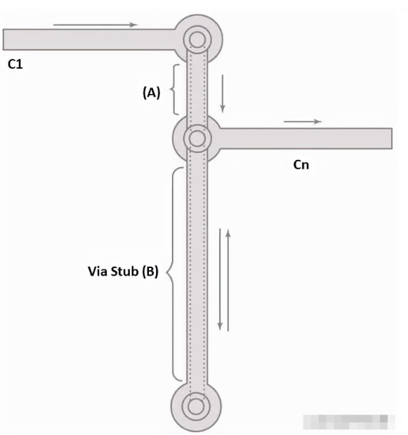
Via stubs are responsible for heavy signal attenuation in PCBs.
Long stubs can act as antennas, increasing issues with meeting EMC standards. Stub traces can also create reflections that negatively impact signal integrity. Pull-up or pull-down resistors for high-speed signals are common sources of stubs. If such resistors are required, route the signals in a daisy-chain fashion.

Avoid stub traces by implementing daisy-chain routing.
9.Signal integrity issues caused by ground bounce
Due to excessive current, the ground reference level of the circuit shifts from the original level. This is due to ground resistance and interconnect resistance such as connecting wires and traces. Therefore, the ground voltage level will be different at different points of the ground. This is called ground bounce because the ground voltage will change with the current.
Techniques to reduce ground bounce:
Implement decoupling capacitor grounding
Include current limiting resistors in series.
Place decoupling capacitors close to the pins.
Proper grounding
The rise time of the signal is a critical parameter in SI issues. To get the desired signal integrity level, we should focus on impedance control, attenuation, ground bounce, propagation delay, and EMI/EMC. Signal integrity measures should be taken during the design phase of the PCB because we cannot come up with new designs every now and then. It is better to deal with it in advance rather than letting it ruin the performance of the device in real time. Check out the post on How to implement a robust PCB design workflow for signal integrity? Collect more information about PCB design signal integrity.