Revolutionizing PCB Prototyping with Additive Manufacturing
Key Takeaways
When exploring modern PCB manufacturing methods, you’ll find that additive manufacturing (AM) fundamentally shifts how prototypes are developed. Unlike traditional subtractive processes, AM allows PCB manufacturing companies to build multi-layer boards layer by layer, eliminating the need for complex etching or drilling. This approach not only reduces PCB manufacturing cost by minimizing material waste but also accelerates turnaround times—critical for startups and enterprises alike.
For low-volume production, AM offers unparalleled flexibility. Imagine creating intricate circuit geometries without expensive tooling adjustments, enabling rapid iterations during product testing. This agility is reshaping the PCB manufacturing business, particularly for applications requiring high-complexity designs like IoT devices or aerospace systems. Cost-prohibitive challenges, such as producing specialized substrates or embedding components, become more manageable with AM’s precision.
Transitioning to additive techniques also addresses bottlenecks in conventional workflows. For instance, companies adopting AM report 50-70% faster prototyping cycles compared to milling or chemical methods. This speed doesn’t compromise quality; advanced AM systems now achieve trace widths under 50µm, rivaling traditional standards.
Looking ahead, the integration of AI-driven design tools with AM platforms promises even greater efficiencies. You’ll see smarter material usage and real-time error correction—key factors driving down PCB manufacturing cost while scaling innovation. As the industry evolves, staying competitive means leveraging these advancements to overcome legacy constraints and unlock new possibilities in electronics development.
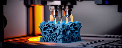
Additive Manufacturing Redefines PCB Prototyping
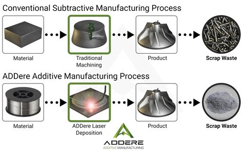
Traditional PCB manufacturing workflows often involve subtractive processes, where excess material is etched away to create circuit patterns. This approach, while reliable, introduces limitations in speed, design flexibility, and material efficiency. Additive manufacturing (AM) flips this paradigm, enabling you to build multilayer boards layer by layer using precision deposition of conductive and insulating materials. By eliminating the need for photomasks and chemical etching, AM reduces PCB manufacturing cost for prototyping stages by up to 70%, according to industry benchmarks.
For PCB manufacturing companies, this shift means faster iterations. Imagine designing a high-complexity board with embedded components or non-planar geometries—features that traditionally require weeks of tooling adjustments. With AM, you can produce functional prototypes in hours, test them, and refine designs the same day. This agility is particularly transformative for startups and R&D teams in the PCB manufacturing business, where time-to-market often dictates competitive success.
The technology also addresses a critical pain point: low-volume production. Conventional methods impose high setup costs, making small batches economically unviable. AM sidesteps this by using the same digital file to print one unit or fifty, without retooling. This scalability allows businesses to validate designs with real-world testing before committing to mass production, reducing financial risks.
Moreover, additive techniques enable unprecedented design freedom. Think of antennas printed directly onto curved surfaces or sensors integrated into flexible substrates—applications that stretch beyond the capabilities of subtractive processes. By leveraging AM, engineers can explore geometries that optimize signal integrity or thermal management, pushing the boundaries of what’s possible in electronics.
As the industry evolves, PCB manufacturing cost savings and speed advantages are driving adoption. Companies no longer need to choose between innovation and affordability; additive manufacturing delivers both. Whether you’re refining a consumer device or prototyping aerospace-grade electronics, AM redefines not just how circuits are made, but how quickly your ideas can transition from concept to reality.
Rapid Prototyping for Complex Multi-Layer PCBs
When developing advanced electronics, you need prototyping solutions that keep pace with intricate multi-layer designs. Traditional PCB manufacturing methods often struggle with complex geometries, requiring multiple iterations and extended lead times. Additive manufacturing eliminates these bottlenecks by enabling direct fabrication of high-density interconnects and embedded components in a single process.
Consider this: conventional subtractive techniques force engineers to wait weeks for prototypes, while 3D-printed boards can be produced in days. This acceleration isn’t just about speed—it reduces PCB manufacturing costs by minimizing material waste and avoiding expensive tooling. For PCB manufacturing companies, this translates to faster client turnarounds and the ability to iterate designs without budget overruns.
| Factor | Traditional PCB Manufacturing | Additive Manufacturing |
|---|---|---|
| Lead Time | 2–4 weeks | 24–72 hours |
| Design Complexity Limit | ≤12 layers | Up to 20+ layers |
| Setup Costs | High (tooling, masks) | Low (digital workflows) |
| Material Waste | 30–40% | <5% |
The flexibility of additive processes allows you to test unconventional architectures—like curved or stacked boards—that were previously impractical. For a PCB manufacturing business, this opens doors to niche markets demanding ultra-compact or thermally optimized layouts. You’re no longer constrained by the limitations of etching or drilling; instead, conductive inks and dielectric materials are deposited layer-by-layer with micron-level precision.
By integrating additive techniques early in the R&D phase, you can identify design flaws before committing to full-scale production. This proactive approach not only slashes PCB manufacturing costs but also ensures compliance with evolving industry standards for signal integrity and miniaturization. As the demand for smarter, smaller devices grows, adopting these methods positions PCB manufacturing companies at the forefront of innovation—ready to tackle tomorrow’s engineering challenges today.
Streamlining Low-Volume Electronics Production
When developing specialized electronics, PCB manufacturing for small batches often faces inefficiencies in traditional processes. Tooling costs, minimum order quantities, and lead times create barriers for innovators needing agile production cycles. Additive manufacturing disrupts this paradigm by enabling on-demand fabrication of circuit boards without molds or etching plates. You no longer need to compromise design complexity to meet volume thresholds set by conventional PCB manufacturing companies—instead, iterative prototypes and functional units can be produced in quantities as low as single digits.
This approach directly addresses PCB manufacturing cost challenges in niche applications. By eliminating tooling expenses and reducing material waste, 3D-printed boards lower breakeven points for pilot runs or customized solutions. For example, a medical device startup can validate ten sensor-embedded boards at 60% lower cost compared to subtractive methods, accelerating time-to-market while preserving capital. The flexibility of additive techniques also allows real-time design adjustments—critical when refining high-frequency or mixed-signal layouts during development.
For PCB manufacturing business models targeting R&D departments or IoT innovators, this capability transforms service offerings. Providers equipped with additive systems can deliver fully functional boards within 48 hours, bypassing weeks-long waits for traditional fabrication. This shift not only strengthens client retention but opens markets for ultra-low-volume production—think aerospace components or AI hardware prototypes. Meanwhile, designers gain freedom to experiment with unconventional geometries or embedded components, knowing physical testing isn’t constrained by prohibitive per-unit costs.
The operational advantages extend beyond speed. Digital inventory management replaces warehousing physical boards, while distributed manufacturing networks enable localized production. As you scale from prototype to pre-series batches, hybrid approaches—combining additive layers with selective conventional processes—offer cost-optimized pathways without sacrificing innovation potential. This fluidity redefines what’s achievable in low-volume electronics, turning what was once a logistical hurdle into a strategic accelerator.
3D Printing’s Role in Accelerating PCB Development
When you need to shrink development timelines for electronic devices, 3D printing offers a paradigm shift in how PCB manufacturing workflows operate. Unlike traditional methods that require weeks for tooling and etching, additive manufacturing enables same-day prototyping of multi-layer boards. This agility lets engineers test design iterations 60–80% faster, compressing what was once a months-long process into days. For PCB manufacturing companies, this means quicker validation of high-frequency or flex-rigid designs before committing to mass production.
"Adopt hybrid 3D-printed PCBs for functional testing—combining conductive inks with dielectric polymers can simulate final product performance at 30% lower PCB manufacturing cost."
The technology’s precision in depositing materials layer-by-layer eliminates the need for chemical etching, reducing material waste by up to 70%. This efficiency is particularly transformative for startups in the PCB manufacturing business, where budget constraints often clash with the demand for complex, small-batch boards. You can now produce antenna arrays or embedded sensor circuits without investing in expensive lithography equipment.
By integrating additive systems into your workflow, supply chain dependencies diminish. Traditional fabrication often involves outsourcing to specialized facilities, but in-house 3D printers allow for on-demand production of prototypes—or even end-use parts for niche applications. This autonomy accelerates debugging cycles and lets you address design flaws before they escalate into costly revisions.
However, success hinges on selecting the right materials. Silver nanoparticle inks and photopolymer resins must meet your application’s thermal and conductivity requirements. Partnering with additive-savvy PCB manufacturing companies ensures compatibility between printed traces and standard soldering processes, bridging the gap between rapid prototyping and industrial-scale production.
Cost-Effective AM Solutions for Circuit Boards
When evaluating PCB manufacturing methods, additive manufacturing (AM) stands out for its ability to slash upfront expenses while maintaining precision. Traditional fabrication often requires costly tooling, chemical etching, and multi-step processes that inflate prototyping budgets. With AM, you eliminate the need for molds or masks, reducing PCB manufacturing cost by up to 70% for low-volume batches. This approach lets smaller teams or startups iterate designs without financial strain, a game-changer for time-sensitive projects.
For PCB manufacturing companies, AM’s material efficiency is transformative. Unlike subtractive methods that waste up to 90% of copper during etching, 3D-printed circuits deposit materials only where needed. This minimizes raw material consumption and aligns with sustainable practices—a growing priority for electronics brands. Additionally, AM systems like aerosol jet printing enable embedded components and non-planar geometries, reducing assembly steps and further trimming labor costs.
Another critical factor is scalability. While traditional workflows struggle with economies of scale for small runs, AM maintains consistent PCB manufacturing cost per unit, even for single-digit orders. This is ideal for R&D labs or businesses testing niche markets. For example, printing a 10-layer board with AM avoids the $5,000–$15,000 tooling fees typical in conventional production, making it viable for customized electronics.
Moreover, AM simplifies supply chains. By adopting in-house 3D printing, your PCB manufacturing business can bypass overseas suppliers and slash lead times from weeks to days. This agility is critical in industries like medical devices or aerospace, where design revisions are frequent. Hybrid solutions—combining AM for prototyping and traditional methods for mass production—offer a balanced cost structure as projects scale.
This financial flexibility doesn’t sacrifice quality. Modern AM systems achieve trace widths under 50µm and compatibility with high-frequency materials, meeting standards for most commercial applications. As you explore AM, consider how its per-unit cost predictability and rapid turnaround align with your product development goals.
Overcoming Traditional PCB Manufacturing Limits
Traditional PCB manufacturing methods often impose rigid constraints that hinder innovation. When relying on subtractive processes, you face prototyping delays due to tooling requirements and minimum order quantities. For PCB manufacturing companies, these bottlenecks escalate PCB manufacturing cost—especially for low-volume runs—while limiting design flexibility for high-density interconnects or unconventional geometries.
Additive manufacturing disrupts this paradigm by enabling direct digital fabrication. Instead of waiting weeks for chemical etching or lamination, you can 3D-print functional prototypes in hours. This eliminates the need for photomasks and drilling templates, slashing upfront expenses for PCB manufacturing business startups and R&D teams. Multi-material printing further bypasses layer alignment issues, allowing embedded components or curved traces that traditional methods can’t achieve.
Material waste presents another critical barrier. Conventional subtractive techniques discard up to 90% of copper substrates during etching—a cost and sustainability liability. Additive processes deposit materials precisely where needed, reducing raw material consumption by 60–80%. This efficiency reshapes PCB manufacturing cost calculations, making small-batch production economically viable without compromising quality.
Thermal management challenges also persist in legacy systems. High-frequency designs demand precise dielectric properties, which additive methods address through graded material deposition. By tailoring conductivity and insulation layer-by-layer, you avoid the performance trade-offs inherent in standardized laminate stacks.
For PCB manufacturing companies transitioning to AM, the shift isn’t just technical—it’s strategic. Early adopters report 70% faster iteration cycles, turning rigid production timelines into agile development opportunities. As material libraries expand, these techniques will continue eroding the barriers that once defined PCB manufacturing’s possibilities.
Additive Techniques for High-Complexity Electronics
When designing advanced electronics, you’re often constrained by the limitations of traditional PCB manufacturing methods—especially when creating boards with intricate geometries, embedded components, or non-planar architectures. Additive techniques bypass these barriers by building circuits layer by layer, enabling unprecedented design freedom. For example, PCB manufacturing companies now leverage inkjet printing or aerosol deposition to produce ultra-fine conductive traces (as narrow as 25 µm) and vertically stacked interconnects, which are nearly impossible with subtractive etching.
This approach shines in applications requiring high-density integration, such as RF devices or IoT sensors. Instead of relying on multi-step lamination processes, additive systems deposit dielectric and conductive materials precisely where needed, reducing material waste and PCB manufacturing cost by up to 40% for low-volume runs. You can also integrate passive components like resistors or antennas directly into the substrate, eliminating assembly steps and improving signal integrity.
For businesses navigating the competitive PCB manufacturing business landscape, these methods offer a strategic edge. Imagine prototyping a 12-layer HDI board with blind vias and thermal management channels in days rather than weeks—without the need for expensive tooling. Additive workflows also support hybrid manufacturing, allowing you to combine 3D-printed circuitry with conventional FR4 substrates for mixed-material designs. While challenges like conductivity consistency remain, advancements in nano-particle inks and laser sintering are closing the performance gap with traditional copper traces.
By adopting additive techniques, you’re not just streamlining production—you’re redefining what’s possible in electronics design. Complex architectures that once demanded compromises in functionality or budget now become viable, accelerating innovation across industries from aerospace to wearable tech.
Future Trends in PCB Prototyping Innovation
As additive manufacturing reshapes the electronics landscape, its influence on PCB manufacturing is poised to accelerate innovation in unprecedented ways. Imagine a future where design iteration cycles shrink from weeks to days, enabled by advanced 3D printing systems that integrate conductive and dielectric materials in a single process. For PCB manufacturing companies, this means breaking free from traditional photolithography constraints, allowing you to prototype high-density interconnects and embedded components with precision unattainable through subtractive methods.
One emerging trend involves AI-driven design optimization tools that work in tandem with additive systems. These platforms analyze your circuit layouts to suggest material-efficient configurations, reducing PCB manufacturing cost by minimizing waste and energy consumption. Hybrid machines combining inkjet printing with laser sintering are also gaining traction, offering multi-layer board fabrication in hours—ideal for low-volume PCB manufacturing business models requiring rapid turnaround.
Another critical development is the rise of sustainable materials for eco-conscious production. Biodegradable substrates and lead-free conductive inks are being optimized for additive processes, aligning with global regulations while maintaining performance. This shift not only future-proofs your prototyping workflows but also opens doors to markets prioritizing environmental responsibility.
However, challenges remain. Scaling additive techniques for mass production requires advancements in print speed and material reliability. Forward-thinking PCB manufacturing companies are already collaborating with chemical suppliers to develop nano-engineered inks that ensure consistent conductivity across complex geometries. As these innovations mature, the gap between prototyping and full-scale production will narrow, redefining how you approach high-mix, low-volume electronics projects.
The integration of smart manufacturing ecosystems will further streamline workflows. Imagine cloud-connected 3D printers that adjust parameters in real-time based on sensor feedback, or blockchain-enabled traceability for every layer of your prototype. These advancements won’t just accelerate development—they’ll transform how you measure quality, manage PCB manufacturing cost, and deliver value in a hyper-competitive industry.
Conclusion
As you explore the evolving landscape of PCB manufacturing, it becomes clear that additive manufacturing is more than a temporary trend—it’s a strategic shift redefining how prototyping and production cycles operate. By integrating this technology, PCB manufacturing companies can bypass traditional constraints like extended lead times and rigid design limitations, enabling you to iterate faster and experiment with high-complexity geometries that were once impractical.
The impact on PCB manufacturing cost is equally transformative. Traditional methods often require expensive tooling and minimum order quantities, but additive techniques allow you to produce low-volume batches economically. This flexibility reduces upfront investments, making it feasible for startups and established businesses alike to test innovations without financial overcommitment. For those in the PCB manufacturing business, this opens doors to niche markets and custom solutions that were previously cost-prohibitive.
Looking ahead, the synergy between additive manufacturing and electronics development will continue to accelerate. As materials and printing precision improve, expect to see broader adoption of multi-layer board fabrication and embedded components—advancements that further compress development timelines. While challenges like material conductivity and certification standards remain, the trajectory points toward a future where PCB manufacturing seamlessly blends speed, affordability, and creativity.
By embracing these innovations now, you position your operations at the forefront of an industry where agility and precision are no longer trade-offs but complementary strengths.
FAQs
How does additive manufacturing reduce prototyping time in PCB development?
By eliminating traditional etching and drilling steps, pcb manufacturing through additive processes builds circuits layer-by-layer. This slashes lead times from weeks to days, letting you test designs faster.
Can complex multi-layer boards be produced cost-effectively with this technology?
Yes. Unlike pcb manufacturing companies relying on subtractive methods, additive systems deposit materials precisely where needed. This reduces waste and lowers pcb manufacturing cost for intricate designs, especially in batches under 100 units.
What limitations of conventional processes does additive manufacturing address?
Traditional pcb manufacturing business models struggle with high tooling costs for low-volume orders. Additive workflows remove molds and masks, enabling economical small runs while maintaining signal integrity in high-frequency applications.
Are there industries benefiting most from additive PCB prototyping?
Medical devices, aerospace, and IoT sectors gain advantages. These fields often require customized geometries and rapid iteration—both strengths of additive techniques that accelerate pcb manufacturing timelines by 40-60%.
How does material selection impact functional performance?
Advanced conductive inks and dielectric polymers now match the thermal stability and conductivity of conventional substrates. This ensures reliability while enabling 3D-embedded components previously unachievable in standard pcb manufacturing.
Ready to Transform Your PCB Development Workflow?
Explore how additive manufacturing can optimize your pcb manufacturing cost and timelines. For tailored solutions from industry-leading pcb manufacturing companies, please click here to consult with specialists today.