In-depth interpretation of PCB, how to repair PCB warping?
PCB circuit board is one of the indispensable components of electronic equipment, and many friends take PCB production and PCB engraving as their own work. In order to enhance everyone’s understanding, this article will introduce the method of repairing PCB warping. If you are interested in PCB or the content of this article, you may wish to continue reading with the editor.
1.PCB
The creator of PCB is Austrian Paul Eisler. In 1936, he first used printed circuit boards in radios. In 1943, Americans mostly used this technology in military radios. In 1948, the United States officially recognized this invention for commercial use. Since the mid-1950s, printed circuit boards have been widely used. Printed circuit boards appear in almost every electronic device. If there are electronic parts in a certain device, they are also embedded in PCBs of different sizes. The main function of PCB is to connect various electronic components to form a predetermined circuit, play the role of relay transmission, and is a key electronic interconnection part of electronic products. It is known as the “mother of electronic products.”
2.PCB warpage repair method
(1)PCB warpage repair in PCB process
In the PCB process, the plate with relatively large warpage is picked out and leveled by a roller leveler, and then enters the next process. Many PCB manufacturers believe that this practice is effective in reducing the warpage rate of PCB finished boards.
(2)PCB finished board warpage repair
For finished products, the warpage is obviously out of tolerance and cannot be leveled by a roller leveler. Some PCB factories put it into a small press (or similar fixture) to press the warped PCB board, and stay for a few hours to ten hours for cold pressing and leveling. From the actual application point of view, the effect of this practice is not very obvious. First, the leveling effect is not great, and second, the flattened board is easy to rebound (that is, warpage recovery).
Some PCB factories will heat the small press to a certain temperature, and then hot press the flattened PCB board. The effect will be better than cold pressing, but excessive pressure will cause wire deformation; if the temperature is too high, defects such as rosin discoloration and its discoloration will occur. Moreover, whether it is cold pressing or hot pressing, it takes a long time (several hours to more than ten hours) to see the effect, and the warping rebound ratio of the flattened PCB board is also very high.
Here, the hot stamping flattening method of the bow mold is recommended. According to the PCB area to be flattened, a simple bow mold is used. Here, two types of leveling operations are proposed.
1) Clamp the warped PCB board into the bow mold and put it into the oven for baking and leveling method:
The warped PCB board is bent to face the curved surface of the mold, and the clamp screws are adjusted to make the PCB board deform and warp in the opposite direction, and then the mold with the PCB board is placed in the oven and heated to a certain temperature for baking. Bake for a while. Under the heating condition, the stress of the substrate gradually relaxes, and the deformed PCB board returns to a flat state. However, the baking temperature should not be too high to avoid discoloration of the rosin or yellowing of the substrate. However, the temperature should not be too low, and it takes a long time to completely relax the stress at a lower temperature.
Generally, the glass transition temperature of the substrate can be used as the reference temperature for baking. The glass transition temperature is the phase transition point of the resin. At this temperature, the polymer chain segments can be rearranged to fully relax the stress of the substrate.
Because the flattening effect is obvious, the advantage of using a bow-shaped mold to flatten is that the investment is small. Ovens can be obtained in PCB factories. The leveling operation is very simple. If the number of seesaws is relatively large, it is enough to make several bow-shaped molds. You can put them in the oven at once. There are fewer molds and the drying time is relatively short (about tens of minutes), so the leveling work efficiency is relatively high.
2) After softening the PCB board, clamp it into the bow-shaped mold and flatten it:
For PCB boards with relatively small warping deformation, the PCB board to be flattened can be placed in an oven that has been heated to a certain temperature (that is, the temperature setting can be determined by referring to the glass transition temperature of the substrate, and the substrate is baked in the oven for a certain time and the softening is observed. Generally, the baking temperature of the glass fiber cloth substrate is higher, and the baking temperature of the paper substrate can be lower; the baking temperature of the thick board can be slightly higher, and the baking temperature of the thin board can be slightly lower.
The baking temperature of the PCB board sprayed with rosin should not be too high. Bake for a certain time, then take a few to a dozen sheets, clamp them into the bow-shaped mold, adjust the pressure screw, and make the PCB board slightly warped and deformed in the opposite direction. After the board is cooled and shaped, The mold can be removed and the flattened PCB board can be taken out.
After the bow mold is flattened, the PCB board has low warping; even after wave soldering, it can basically remain flat; and the impact on the appearance and color of the PCB board is also small.
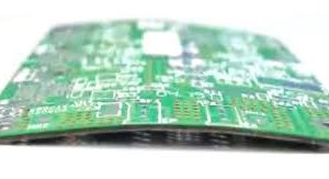
PCB board warping is a headache for PCB manufacturers. It not only reduces production, but also affects delivery time. If an arc mold is used for heat leveling, and the leveling process is reasonable and appropriate, the warped PCB board can be leveled to solve the delivery problem.
The above is the PCB-related content brought by the editor this time. Through this article, I hope everyone has a certain understanding of PCB. If you like this article, you may wish to continue to pay attention to our website. The editor will bring more exciting content later. Finally, thank you very much for reading, have a nice day!