How to control a small UPS power supply by controlling the corresponding DC-DC module
Introduction
This type of small intelligent UPS power supply is mainly used in low-voltage occasions such as the communications industry, medical equipment and mobile robots. It has the characteristics of reliable operation, low noise and low energy consumption. At present, many foreign universities and companies are conducting research and trial production on this type of UPS, and have made some progress in small AC UPS power supplies. However, the relevant research conducted in China is still in its infancy.
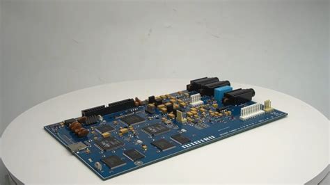
Unlike most UPS power supplies with AC output, the small UPS power supply proposed in this paper directly obtains DC output by controlling the corresponding DC-DC module, avoiding energy loss during the conversion process. The embedded design concept is adopted in the system design, and the main control chip and the peripheral functional circuit are integrated into the same circuit board. The software and hardware work together to realize the intelligent management of UPS and greatly reduce the size of the system.
1 Hardware system
1.1 System overview
According to the project needs, the design uses 110 V/50Hz AC as the mains input, and converts 110V AC into 12 V DC through the switching power module. At the same time, the module has a built-in mains detection module to generate a mains power failure signal and transmit the signal to the main control chip. The mains power is converted by the switching power supply AC-DC to obtain a 12 V DC output and supplied to the load through the LTC4256 hot-swap protection module. At the same time, the DC output is regulated by the LTC1512 charging module to charge the lithium battery pack. When the system works in the battery pack power supply mode, the lithium battery pack provides 12 V DC power to the load through the LTC3780 discharge module.
1.2 Main control chip
In order to improve the integration of the system, the design uses the C8051F320 with an internal integrated AD conversion function unit as the main control chip. The chip contains two external interrupt sources (INT0, INT1) and a programmable counter array (PCA), which can monitor multiple I/O signals and generate square wave control signals at the same time.
The main control chip continuously reads the voltage, temperature, and charging current of the lithium battery pack to obtain the current operating status of the system. When the mains power failure signal is captured, the main control chip quickly sends a working signal (high level) to LTC3780 and sends a shutdown signal (low level) to LTC1512, thereby realizing uninterrupted power supply to the load; when the mains call signal is captured, the main control chip gives the opposite logic level and switches to the mains power supply state.
1.3 Mains power detection module
In order to achieve isolation protection for the main control chip and other peripheral chips, the mains power detection module connects the mains power failure signal to the main control chip through the PC817 type optocoupler: when the mains power is normally supplied, under the drive of the photosensitive diode, the corresponding pin of the main control chip is directly grounded and set low; when the mains power is lost, the optocoupler is disconnected, and the corresponding pin is set high by the 3.3 V power supply. The main control chip monitors the change of the logic level on the pin through the interrupt program to obtain the state of the mains power supply and control the UPS power supply to work in the corresponding state.
1.4 Power management module
The power management module consists of a power selection unit and a voltage stabilizing chipset. The design uses the power selection chip LTC4416 to realize internal power selection. The switching power supply output is the main power supply, and the lithium battery pack is the slave power supply. Its working mode is: when the main power supply is supplied by the mains, the LTC4416 determines that the main power supply is normal through the E1 pin; when the output voltage of the switching power supply is lower than Vf a iLTC4416 determines that the main power supply is faulty, and selects the lithium battery pack to supply power to the system. The power selection circuit not only ensures the normal power supply inside the system, but also increases the working time of the battery pack. The voltage regulator chip group stabilizes the selected power supply to 5 V and 3.3 V respectively, and provides it to the corresponding modules.
1.5 Backup lithium battery pack
The UPS power supply uses a 14.4 V, 3.3 Ah rechargeable lithium battery pack as a backup battery pack, and its maximum charging voltage is 17.4 V. The battery pack integrates a control chip. After power supply, the control chip can generate a charging completion signal, a discharge end signal, and the battery pack temperature.
1.6 Charging module and discharging module
The charging module with LTC1512 as the core converts 12 V DC input into 16.8 V constant current output to charge the battery pack through voltage and current feedback regulation. When the battery pack is powered, the discharging module with LTC3780 as the core stabilizes the battery pack output to 12 V and provides it to the load.
In order to realize the intelligent management of UPS, the system needs to monitor the battery pack voltage and charging current. The battery pack voltage is measured by dividing and filtering the voltage and sending it to the AD conversion unit of the main control chip to process the current voltage value. The charging current is obtained by sending the voltage at both ends of the sampling resistor to the ADC unit to convert the voltage difference, and then derive the current value.
1.7 Hot-swap module
Hot-swap protection is live plug-in protection, which allows users to remove and replace components such as hard disks, power supplies or boards without shutting down the system or cutting off the power supply. One of the advantages of this UPS power supply is that it integrates a hot-swap protection module with LTC4256 as the core, thereby improving the system’s timely recovery capability, scalability and flexibility to disasters. In addition, LTC4256 can also suppress output ripple and improve power quality.
Switching power supply is one of the commonly used power supply methods in modern electronic equipment. It has the advantages of high efficiency, small size, good stability, etc., and is widely used in various electronic products. However, for beginners, designing and debugging switching power supplies can be a challenging task. This article will start from scratch and introduce how to design and debug switching power supplies step by step.
Understand the basic principles of switching power supplies
Before designing a switching power supply, you must first understand the basic principles of switching power supplies. The switching power supply adjusts the input power supply through the switching action of the switching tube, thereby outputting the required voltage and current. Its basic components include input filter circuit, rectifier circuit, conversion circuit, output filter circuit, etc. For beginners, it is recommended to first learn the relevant theoretical knowledge and have a clear understanding of the working principle of the switching power supply.
Choose the right devices and components
When designing a switching power supply, it is crucial to choose the right devices and components. For example, select appropriate switching tubes, transformers, capacitors, inductors and other components to ensure the performance and stability of the power supply. In addition, it is necessary to select appropriate control circuits and protection circuits according to design requirements to improve the reliability and safety of the power supply.
After selecting the devices and components, you can start circuit design and simulation analysis. Use circuit design software to draw the schematic diagram of the switching power supply, and perform simulation analysis to verify the performance and stability of the circuit. Through simulation analysis, problems in the circuit can be discovered and solved in a timely manner, improving the efficiency and accuracy of the design.
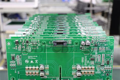
PCB design and layout and wiring
After completing the circuit design and simulation analysis, the next step is PCB design and layout and wiring. Reasonable PCB layout and wiring can effectively reduce the electromagnetic interference and noise of the circuit and improve the anti-interference ability and stability of the circuit. Therefore, when designing PCB, it is necessary to pay attention to the specifications and techniques of layout and wiring to ensure the performance and reliability of the circuit.
Perform experimental verification and debugging optimization
After completing the PCB design and layout and wiring, the next step is to perform experimental verification and debugging optimization. The designed PCB board is processed and manufactured, and experimental verification is performed to check the working status and performance parameters of the circuit. During the experimental verification process, some problems may arise, and timely debugging and optimization are required to find and solve the problems and ensure the normal operation of the circuit.
Summarize and share experience
Finally, after completing the design and debugging of the switching power supply, you can summarize the whole process and share experience. Summarizing experience can help us better understand and master the design and debugging skills of the switching power supply, and provide reference and reference for future design work. At the same time, you can also communicate and learn with others by sharing experience and make progress together.
Through the above six steps, we can gradually learn and master the design and debugging skills of the switching power supply, so as to design a switching power supply with stable performance and high reliability. Although there may be some challenges in designing and debugging the switching power supply, as long as you have patience and courage, I believe everyone can complete this task. I hope this article can help you, and I wish you success in the design and debugging of the switching power supply!