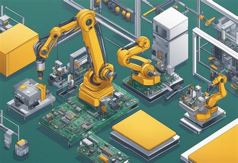
PCB Assembly Drawing Essentials for Manufacturing Precision
Key Takeaways
Effective PCB assembly requires meticulous attention to design documentation, particularly in assembly drawings that serve as blueprints for manufacturing Below are critical insights to ensure precision in PCBA production:
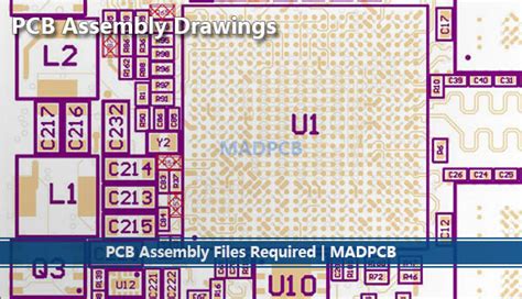
1 Design Clarity: A well-structured PCB assembly drawing must include unambiguous annotations for component placement, orientation, and polarity Missing details can lead to misalignment or solder defects
2 Tolerance Alignment: Specify mechanical and electrical tolerances for components, holes, and traces For example:
| Parameter | Recommended Tolerance | Impact of Deviation |
|---|---|---|
| Component Placement | ±01mm | Signal Integrity |
| Drill Hole Diameter | ±005mm | Mechanical Fit |
| Solder Mask Clearance | ±007mm | Short Circuits |
3 Quality Anchors: Integrate DFM (Design for Manufacturing) checks early to identify high-risk areas like insufficient pad spacing or thermal imbalances
Tip: Use CAD tools to automate tolerance validations and generate layer-specific views for complex PCBA layouts This reduces human error during manual reviews
4 Error Prevention: Cross-reference the assembly drawing with the BOM (Bill of Materials) to ensure part-number consistency and revision control Discrepancies here account for 30% of prototyping delays
By prioritizing these elements, manufacturers can avoid costly rework and achieve first-pass success in PCB assembly Transitioning seamlessly into component placement strategies, the next section explores spatial optimization techniques for high-density boards
PCB Assembly Drawing Design Fundamentals
Effective PCB assembly design begins with establishing clear documentation that bridges schematic concepts and physical manufacturing At its core, a PCBA drawing must communicate precise spatial relationships, material specifications, and functional requirements to ensure seamless translation from design to production
Central to this process is defining component placement guidelines, which dictate how parts like resistors, ICs, and connectors are oriented on the board Proper spacing between components minimizes signal interference and simplifies soldering processes during PCB assembly Designers must also integrate reference designators and polarity markers to eliminate ambiguity, particularly for surface-mount devices (SMDs) where alignment errors can compromise functionality
A critical yet often overlooked aspect involves specifying tolerances for hole sizes, trace widths, and solder mask clearances For instance, a ±01mm tolerance on pad dimensions ensures compatibility with automated pick-and-place machinery, reducing misalignment risks in PCBA workflows Additionally, layer stack-up details and copper weight annotations guide manufacturers in maintaining impedance control and thermal performance
To enhance manufacturability, designers should adopt unified symbol libraries within CAD tools, ensuring consistency across schematics and assembly drawings This alignment prevents discrepancies between electrical and mechanical data, which are a common source of rework Furthermore, including fiducial markers and tooling holes in the design aids in precise board alignment during high-volume production runs
Transitioning to fabrication-ready documentation requires balancing detail with clarity Overloading drawings with redundant annotations can obscure critical information, while omitting key specifications risks costly misinterpretations By adhering to standardized drafting practices and validating designs through Design-for-Manufacturing (DFM) checks, engineers create PCB assembly drawings that align technical intent with practical execution, laying the groundwork for defect-free electronic assemblies
Component Placement Strategies for Precision
Effective PCB assembly relies on meticulous component placement to balance electrical performance, manufacturability, and long-term reliability Signal integrity and thermal dissipation are primary considerations when positioning components on a PCBA High-speed traces, for instance, require shorter paths between critical components like microcontrollers and memory modules to minimize electromagnetic interference (EMI) Grouping analog and digital sections separately, with adequate spacing, reduces cross-talk risks while optimizing grounding schemes
Orientation consistency is another cornerstone of precision placement Aligning polarized components—such as diodes or electrolytic capacitors—in uniform directions reduces errors during automated assembly Additionally, heavy components like transformers or heat sinks should be positioned near board supports to prevent mechanical stress during thermal cycling For high-density designs, staggered placement of smaller surface-mount devices (SMDs) ensures adequate clearance for soldering and inspection
Thermal management demands strategic placement of heat-generating components Power regulators or RF modules, for example, should be isolated from temperature-sensitive parts like crystal oscillators Integrating thermal relief patterns in copper pours and placing these components near board edges enhances airflow efficiency When combined with tolerance specifications (discussed later), this approach mitigates warping risks during reflow soldering
A critical yet often overlooked aspect is design-for-testability Positioning test points along key signal paths enables seamless in-circuit testing (ICT) without obstructing rework access Similarly, fiducial markers must be placed in asymmetrical locations to aid pick-and-place machines in accurate alignment By adhering to these strategies, PCB assembly workflows achieve higher first-pass yields while meeting stringent quality control benchmarks
Transitioning from placement to manufacturing readiness requires harmonizing these strategies with Design-for-Manufacturing (DFM) principles The next section explores how tolerance specifications bridge the gap between theoretical design and practical execution
Tolerance Specifications in PCB Manufacturing
Precision in PCB assembly relies heavily on defining and adhering to critical tolerance specifications across design and production phases These specifications govern dimensional accuracy, component alignment, and material behavior, ensuring that PCBA (Printed Circuit Board Assembly) outputs meet both functional and reliability requirements
Dimensional tolerances for features like drill hole diameters, pad sizes, and trace widths are foundational For example, drilled holes for through-hole components typically require ±01mm precision to avoid misalignment during PCB assembly, while surface-mount pads demand tighter ±005mm tolerances to prevent solder bridging Similarly, copper trace width variations must stay within ±10% to maintain consistent impedance in high-frequency circuits
Component placement tolerances are equally vital Automated pick-and-place systems in PCBA workflows often operate at ±0025mm accuracy, but design files must specify allowable deviations for rotational orientation (±1–2°) and positional offsets (±01mm) Overlooking these details risks misaligned connectors or insufficient solder joint coverage, particularly in fine-pitch ICs or BGAs
Material-related tolerances, such as thermal expansion coefficients (CTE) of substrates and solder masks, ensure structural integrity under thermal cycling For instance, FR-4 substrates with a CTE tolerance of 14–16 ppm/°C minimize warping during reflow soldering, while solder mask thickness variations below ±5µm prevent uneven curing
To enforce compliance, designers should reference industry standards like IPC-6012 (performance specifications for rigid PCBs) and IPC-A-610 (acceptability criteria for PCBA) These frameworks provide measurable thresholds for annular ring integrity, solder fillet geometry, and via wall plating—each directly tied to manufacturability
Statistical process control (SPC) tools and automated optical inspection (AOI) systems are often integrated into PCB assembly lines to monitor tolerance adherence in real time For high-reliability applications, such as aerospace or medical devices, designers may adopt six-sigma methodologies to reduce process variability below 15σ
Balancing tighter tolerances with cost efficiency remains a key challenge Over-specifying requirements can escalate PCBA expenses by 20–30%, while under-specifying risks field failures A collaborative approach—aligning design intent with fabrication capabilities—ensures optimal tolerance allocation without compromising quality
Quality Control Protocols for Flawless Assembly
Implementing rigorous quality control protocols is critical to achieving defect-free outcomes in PCB assembly These protocols begin with design verification, where PCBA documentation undergoes automated checks to ensure alignment between schematic symbols, footprint geometries, and bill-of-materials (BOM) specifications Advanced design rule checks (DRCs) flag potential issues like pad-to-trace spacing violations or mismatched component orientations before manufacturing commences
During the pcb assembly process, automated optical inspection (AOI) systems scan solder joints and component placements against the assembly drawing’s tolerance specifications, detecting deviations as small as 001mm For high-density interconnects (HDIs), X-ray inspection complements AOI by verifying hidden connections such as ball grid array (BGA) soldering integrity Post-assembly, functional testing simulates real-world operating conditions to validate electrical performance, with test coverage metrics ensuring 95%+ fault detection
A tiered non-conformance management system categorizes defects by severity, enabling prioritized corrective actions Critical flaws like short circuits trigger immediate process halts, while minor deviations initiate root-cause analyses using statistical process control (SPC) data To maintain traceability, serialized lot tracking links each PCBA unit to its inspection records, material certifications, and revision-controlled assembly drawings
Proactive supplier quality audits further reinforce reliability by validating component authenticity and parametric consistency By integrating these protocols with pcb assembly workflows, manufacturers reduce rework rates by up to 40% while achieving first-pass yield improvements exceeding 25% Continuous feedback loops between quality teams and design engineers ensure iterative refinements to both assembly processes and documentation standards
CAD Integration in Assembly Documentation
Modern PCB assembly processes demand seamless coordination between design intent and manufacturing execution, making CAD integration indispensable Advanced computer-aided design tools bridge the gap between schematic layouts and physical PCBA production by automating critical documentation steps For instance, software like Altium Designer or AutoCAD Electrical enables designers to embed tolerance specifications, component orientation markers, and layer stack-up details directly into assembly drawings, ensuring machine-readable accuracy for fabrication partners
A key advantage lies in the ability to generate Gerber files and pick-and-place data directly from CAD platforms, minimizing manual interpretation errors By standardizing symbols for surface-mount devices (SMDs) and through-hole components, these tools enforce consistency across bill of materials (BOM) annotations and assembly layer views Additionally, 3D modeling features allow manufacturers to perform virtual fit checks, identifying potential collisions between oversized parts and adjacent circuitry before prototyping
Effective integration also streamlines revision control When design updates occur—such as adjusting a footprint or rerouting a power plane—the linked pcb assembly documentation auto-synchronizes, preserving alignment between schematic revisions and manufacturing instructions This dynamic linkage reduces discrepancies that often lead to rework cycles or field failures
To maximize efficiency, engineers should configure CAD export settings to include fiducial markers and panelization guides, which are critical for automated optical inspection (AOI) systems Embedding IPC-7351 compliance checks within the design workflow further ensures that PCBA layouts meet global manufacturability standards By leveraging parametric constraints in CAD software, teams can enforce minimum clearance thresholds and solder mask apertures, translating design rules into enforceable production parameters
As the industry shifts toward high-mix, low-volume production, robust CAD-driven documentation becomes a cornerstone for maintaining precision across diverse pcb assembly projects This approach not only accelerates time-to-market but also establishes a auditable trail for quality assurance protocols—a necessity in aerospace, medical, and automotive electronics sectors where traceability and process validation are non-negotiable
Thermal Management via Layout Optimization
Effective thermal management begins with strategic component placement in PCB assembly design High-power components like power regulators and processors generate concentrated heat, requiring deliberate spacing from thermally sensitive elements By grouping heat-generating parts in zones with optimal airflow and isolating them from analog circuits, designers prevent thermal interference that degrades signal integrity
A key tactic involves using thermal vias—plated holes that transfer heat from surface-mounted devices to inner copper layers or heatsinks When paired with copper pours acting as heat spreaders, these vias reduce localized hot spots by up to 30%, as demonstrated in industrial PCBA applications For multilayer boards, dedicating inner layers to solid ground planes enhances thermal conductivity while maintaining EMI shielding
Trace routing also impacts heat dissipation Widening power traces lowers current density, minimizing resistive heating—a critical factor in high-current PCB assembly designs Implementing 45-degree angled traces at component junctions further reduces thermal stress points compared to traditional right-angle configurations
Material selection completes the thermal management equation Substrates with higher glass transition temperatures (Tg) and metal-core boards are increasingly adopted for PCBA projects requiring prolonged thermal stability Simulation tools like ANSYS Icepak enable designers to model heat distribution pre-production, aligning with Design-for-Manufacturing (DFM) principles to avoid rework
By integrating these layout strategies, engineers ensure reliable operation across temperature extremes—a non-negotiable requirement for automotive and aerospace PCB assembly standards This systemic approach to thermal optimization directly correlates with improved mean time between failures (MTBF) in field-tested electronics
Design-for-Manufacturing Best Practices
Implementing Design-for-Manufacturing (DFM) principles in PCB assembly ensures seamless transitions from design to production while minimizing costly revisions A critical starting point involves selecting components that balance performance with manufacturability—prioritizing standardized package sizes and avoiding obsolete parts that delay PCBA workflows For instance, surface-mount devices (SMDs) with fine-pitch leads demand precise pad geometries, which must align with the fabricator’s capabilities to prevent soldering defects
Optimizing component placement goes beyond spatial efficiency High-frequency or heat-sensitive parts, such as voltage regulators, require strategic distancing from thermal sources to mitigate signal degradation Incorporating thermal relief pads in power planes and using symmetrical copper pours around BGAs (Ball Grid Arrays) enhance heat dissipation while maintaining mechanical stability during reflow soldering Additionally, adhering to minimum clearance rules (e.g., 02mm between traces and board edges) prevents manufacturing tool interference
Collaboration with PCB assembly partners early in the design phase is non-negotiable Sharing preliminary Gerber files and assembly drawings for DFM analysis uncovers potential pitfalls like insufficient solder mask expansion or misplaced fiducial markers For example, a missing solder thief pad near a QFN (Quad Flat No-lead) component could lead to tombstoning Embedding IPC-2221 and IPC-A-610 standards directly in documentation clarifies acceptability thresholds for annular rings and solder fillets
To streamline PCBA processes, designers should integrate automated DFM checks within CAD tools These tools flag violations such as unconnected nets or mismatched hole-to-pad ratios, reducing human error Including a dedicated assembly layer in drawings—annotating polarity, pin-one indicators, and orientation for ICs—eliminates ambiguity during pick-and-place operations
Finally, validating designs through prototype builds identifies latent issues like component shadowing in wave soldering Iterative testing under real-world conditions ensures that PCB assembly outcomes meet both electrical and mechanical tolerances specified in the drawings By embedding DFM checks at every stage, engineers achieve first-pass success rates exceeding 90%, slashing time-to-market for complex electronics

Error Prevention in PCB Assembly Drawings
Effective error prevention in PCB assembly drawings begins with comprehensive design validation and adherence to standardized documentation practices A single oversight in component labeling, solder mask clearances, or drill hole alignment can cascade into costly manufacturing defects To mitigate risks, engineers must prioritize design-for-manufacturing (DFM) principles, ensuring that every layer of the PCBA documentation aligns with fabrication capabilities
Implementing automated design rule checks (DRC) within CAD tools serves as the first line of defense against geometric mismatches and footprint errors For instance, validating pad-to-trace spacing against the manufacturer’s tolerance specifications prevents short circuits during solder reflow Additionally, clear polarity markings for components like diodes and electrolytic capacitors eliminate orientation-related assembly faults
Another critical step involves annotating critical dimensions with unambiguous callouts Specifying IPC Class 2/3 standards directly on the drawing clarifies quality expectations, reducing interpretation variances between design and production teams For complex PCB assembly projects, cross-referencing the bill of materials (BOM) with component placement diagrams ensures consistency in part numbers and package types
Adopting revision control protocols is equally vital Version tracking prevents outdated drawings from entering production, while cloud-based collaboration platforms enable real-time updates across stakeholders For high-density PCBA designs, incorporating thermal relief patterns and copper balance indicators minimizes warpage risks during thermal cycling
Finally, establishing multistage review checklists that cover footprint accuracy, layer stack alignment, and fiducial marker placement reinforces accountability Combining automated verification with human oversight creates a robust error-detection framework, ensuring that PCB assembly drawings translate seamlessly into reliable electronic products
Conclusion
In the realm of modern electronics manufacturing, PCB assembly documentation serves as the cornerstone for achieving precision and repeatability A well-executed PCBA drawing transcends mere technical illustration—it acts as a contractual blueprint that harmonizes design intent with manufacturing realities By integrating tolerance specifications, thermal management considerations, and Design-for-Manufacturing (DFM) principles, engineers bridge the gap between theoretical layouts and practical execution
The efficacy of PCB assembly workflows hinges on meticulous attention to component placement strategies and quality control protocols Tools like CAD software ensure dimensional accuracy, while standardized annotations eliminate ambiguities that could lead to costly rework Importantly, error prevention mechanisms embedded within assembly drawings—such as clear polarity markings and solder mask definitions—reduce defects during high-volume production
As manufacturing evolves, the role of PCBA documentation expands to accommodate emerging technologies like embedded components and advanced substrate materials Engineers must prioritize collaboration with fabrication partners to refine tolerances and validate thermal dissipation models Ultimately, a robust assembly drawing is not static; it evolves alongside design iterations, ensuring that every revision aligns with both performance goals and industry compliance standards
By treating PCB assembly drawings as living documents—continuously optimized through feedback loops and post-production audits—manufacturers safeguard product integrity while accelerating time-to-market In an era where miniaturization and signal integrity dominate design challenges, precision in documentation remains the linchpin of flawless electronic outcomes
Frequently Asked Questions
What information should a comprehensive PCB assembly drawing include?
A complete PCB assembly drawing must specify component placement coordinates, orientation markers, reference designators, and PCBA-specific requirements like solder mask openings It should detail IPC-610 compliance standards, layer stack-up configurations, and critical tolerance zones for high-precision components
How does component placement affect manufacturing efficiency?
Strategic placement reduces solder bridging risks and optimizes automated pick-and-place operations Components requiring thermal management should be positioned away from heat-sensitive parts, while connectors and test points must align with PCBA testing equipment interfaces
What tolerance standards govern PCB assembly drawing accuracy?
Critical dimensions typically follow ±015mm positional tolerances for SMD components and ±02mm for through-hole parts High-density PCB assembly projects may require ±005mm precision, necessitating ASME Y145 geometric dimensioning callouts
Why are design-for-manufacturing (DFM) checks vital in assembly drawings?
DFM analysis identifies solderability issues, component clearance conflicts, and thermal expansion mismatches early Over 63% of PCBA rework costs stem from preventable DFM oversights, making adherence to IPC-7351 land pattern guidelines essential
How should revisions be managed in assembly documentation?
Implement revision control tables with clear timestamps and ECO (Engineering Change Order) references Cloud-based PCB assembly platforms now automate version tracking, ensuring manufacturers always access the latest approved fabrication data
Can automated optical inspection (AOI) replace manual drawing reviews?
While AOI systems detect solder defects and missing components, they cannot verify drawing-to-BOM consistency Hybrid verification combining AI-driven anomaly detection with manual first-article inspection delivers 987% defect-free PCBA outcomes
Optimize Your Assembly Process Today
For expert guidance on translating PCB assembly drawings into manufacturable designs, please click here to access our engineering team’s proven PCBA optimization toolkit