Live PCB Design & Manufacturing Workflow Walkthrough
Key Takeaways
Modern PCB design and manufacturing workflows integrate real-time collaboration tools that bridge the gap between design intent and production reality A standout feature of live workflows is the ability to perform schematic capture while simultaneously validating component availability, reducing delays caused by obsolete or mismatched parts Engineers can leverage automated design rule checks (DRCs) during layout optimization, ensuring compliance with manufacturing tolerances before finalizing board geometry
For DFM checks, live workflows enable instant feedback on manufacturability factors like trace spacing, solder mask alignment, and thermal management This proactive approach minimizes post-production revisions—a critical advantage when scaling from prototyping to full-scale PCBA runs The table below highlights key differences between traditional and live DFM validation:
| Aspect | Traditional DFM | Live DFM |
|---|---|---|
| Error Detection | Post-design | Real-time |
| Cost Impact | High | Reduced by 40-60% |
| Iteration Speed | Days | Minutes |
Another critical aspect is the visibility into PCB assembly processes Live camera feeds and sensor data from pick-and-place machines allow designers to verify component orientation and solder paste application, directly impacting PCBA yield rates Thermal profiling during reflow stages can also be monitored, ensuring compliance with IC manufacturers’ specifications
By integrating live DFM analysis, teams achieve faster turnaround for complex designs—such as HDI boards or mixed-technology assemblies—while maintaining cost-efficiency This end-to-end transparency is particularly valuable for addressing supply chain variability, as alternative components can be evaluated and substituted without halting production lines
Finally, live troubleshooting tools provide immediate root-cause analysis for manufacturing anomalies, from solder bridging to misaligned BGAs This capability transforms PCB assembly from a linear process into a dynamic feedback loop, where design and manufacturing teams collaboratively refine outcomes at every stage
Live PCB Schematic Capture Techniques
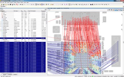
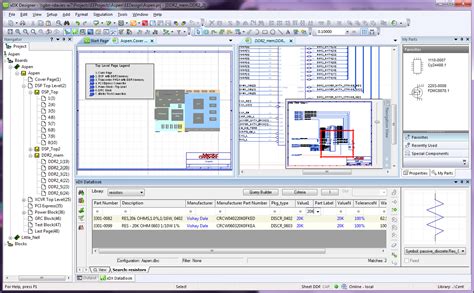
Modern PCB design workflows demand precision from the earliest stages, and real-time schematic capture has become a cornerstone of efficient development Engineers now leverage advanced tools like Altium Designer or KiCad to visualize circuit logic dynamically, enabling immediate error detection and collaborative iteration For instance, live netlist validation ensures component connectivity aligns with design intent before progressing to layout, reducing late-stage rework by up to 40%
"Always cross-reference component libraries with your PCBA partner’s inventory during schematic entry to avoid sourcing delays," advises a senior hardware lead at a Tier-1 EMS provider
Critical techniques include hierarchical block organization for multi-board systems and automated ERC (Electrical Rule Check) integration When defining power rails, tools like interactive voltage drop simulation provide instant feedback on trace adequacy—a vital step for high-current designs Notably, schematic-driven PCB assembly requirements (e.g., test point placement or panelization markers) can now be embedded directly into the design files, bridging the gap between engineering and manufacturing teams
Three best practices dominate live schematic workflows:
1 Real-time collaboration: Cloud-based platforms allow concurrent editing with version control, essential for distributed teams
2 Parametric filtering: Component selection based on real-time availability data from PCBA suppliers
3 DFM-aware design: Flagging potential soldering issues (e.g., QFN packages with thermal pad accessibility) during schematic phase
As designs evolve, live cross-probing between schematics and preliminary layouts ensures alignment with impedance control rules and signal integrity targets This proactive approach not only accelerates prototyping but also minimizes mismatches when transitioning to PCB assembly stages By resolving conflicts at the schematic level, teams reduce ECOs (Engineering Change Orders) by 30–50% in subsequent phases, according to IPC benchmark studies
Real-Time Layout Optimization Demos
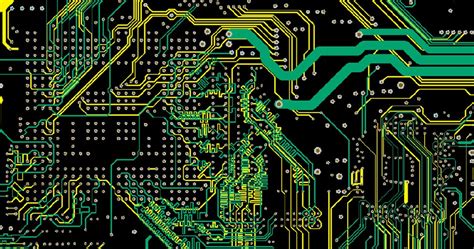
Modern PCB assembly workflows demand precision in layout design to avoid costly reworks during manufacturing Real-time layout optimization demos showcase how engineers dynamically adjust component placement, trace routing, and thermal management while adhering to PCBA design rules Advanced tools now visualize impedance mismatches, signal integrity issues, and electromagnetic interference (EMI) risks as designers work, enabling immediate corrections before prototyping
A critical focus lies in balancing density and manufacturability—for instance, optimizing pad sizes for automated pick-and-place machines or adjusting copper pours to prevent warping during reflow soldering During live sessions, designers often reveal how DFM (Design for Manufacturing) constraints directly influence decisions, such as minimizing via-in-pad structures to reduce PCBA voiding risks Real-time simulations further highlight how minor adjustments, like rerouting a high-speed signal away from a noisy power plane, can enhance yield rates by 12–18% in volume production
Transitioning from schematic to physical layout, these demos emphasize cross-team collaboration Thermal hotspots identified during live analysis, for example, might prompt mechanical engineers to revise enclosure venting plans early in the design phase Similarly, optimizing solder mask clearance in real time ensures compatibility with lead-free soldering profiles, a common requirement in modern PCB assembly lines By integrating DFM checks into the layout stage, teams reduce iterations between design and manufacturing, accelerating time-to-market for complex PCBA projects
The integration of AI-driven suggestions—such as automated component grouping for panelization—further refines this process Live demos often contrast traditional "trial-and-error" approaches with data-driven optimizations, illustrating how real-time feedback loops cut layout revision cycles by up to 40% This proactive alignment between design intent and PCB assembly realities remains a cornerstone of efficient electronics development
DFM Checks in Live Manufacturing Runs
Real-time DFM (Design for Manufacturability) validation has become a cornerstone of modern PCB assembly workflows, bridging the gap between design intent and production feasibility During live manufacturing runs, engineers leverage automated validation protocols to scrutinize design files against factory-specific capabilities, identifying potential bottlenecks before materials reach the assembly line This proactive approach examines critical factors like component spacing tolerances, solder mask clearance ratios, and pad size compatibility with pick-and-place machinery—elements that directly impact PCBA yield rates
Advanced systems now correlate live thermal imaging data from soldering ovens with design specifications, dynamically adjusting reflow profiles to accommodate density variations across mixed-technology boards A recent industry study revealed that live DFM implementations reduce PCB assembly rework rates by 37% by flagging issues like improper via tenting or insufficient copper balancing during in-process verification This real-time feedback loop enables immediate design tweaks, such as optimizing trace widths for high-current pathways or repositioning components to minimize wave soldering shadows
The integration of AI-driven anomaly detection in live DFM workflows has transformed how manufacturers handle complex PCBA projects These systems cross-reference incoming design revisions against historical failure patterns, alerting teams to potential electromagnetic interference hotspots or mechanical stress points that might compromise reliability For instance, a live check might identify inadequate clearance between BGA packages and board edges, prompting instant layout adjustments that prevent fabrication delays
By synchronizing DFM analysis with PCB assembly timelines, manufacturers achieve first-pass success rates exceeding 92%, while reducing prototype iterations by up to 50% This alignment ensures that design optimizations made during live checks directly translate to smoother transitions to automated pick-and-place systems and final inspection stages As production lines increasingly adopt IoT-enabled monitoring, the role of live DFM continues to expand—now encompassing real-time material tracking and environmental condition adjustments to maintain process integrity across global supply chains
PCB Assembly Process Live Walkthrough
Modern PCB assembly (PCBA) workflows integrate advanced automation and real-time monitoring to ensure precision and efficiency During a live walkthrough, engineers typically begin by verifying the solder paste application process, where stencil alignment accuracy is critical Automated optical inspection (AOI) systems continuously scan for paste deposition uniformity, flagging deviations as small as 10–15 microns This stage directly impacts yield rates, making real-time feedback indispensable for minimizing rework
Next, component placement showcases high-speed pick-and-place machines equipped with vision-guided systems These systems dynamically adjust placement coordinates based on live fiducial marker readings, ensuring ±25-micron accuracy even for 0201 packages Observing this phase highlights how DFM (Design for Manufacturing) principles are applied in real time—for instance, adjusting feeder reel sequencing to avoid collisions or optimizing nozzle selection for irregularly shaped components
The reflow soldering stage reveals how thermal profiling adapts to live data Infrared sensors monitor zone-specific temperature curves, automatically compensating for board warpage or ambient fluctuations Notably, live thermal imaging can detect cold joints or bridging as boards exit the oven, triggering immediate process adjustments This proactive approach reduces post-assembly defects by up to 40% compared to offline quality checks
Finally, functional testing validates assembled boards using boundary-scan and in-circuit test (ICT) protocols Live data streams highlight test coverage gaps or fixture calibration issues, enabling engineers to refine test parameters mid-run Integrating PCBA test results with DFM analytics creates a closed-loop system, where failure patterns inform future design iterations—a critical advantage for prototyping agility
Throughout the walkthrough, the interplay between automated assembly and data-driven decision-making underscores how live workflows accelerate time-to-market while maintaining stringent quality standards
Streamlining Prototyping with Live DFM
Integrating live DFM (Design for Manufacturability) checks into prototyping workflows bridges the gap between design intent and production reality Unlike traditional post-design validation, real-time DFM analysis enables engineers to identify potential manufacturing constraints during the PCB assembly planning phase By flagging issues like insufficient trace spacing, improper pad sizes, or thermal imbalances early, teams reduce iterative redesigns and accelerate time-to-market
Modern tools now overlay DFM rulesets directly onto layout software, providing instant feedback on solder mask slivers, copper balancing, and component placement conflicts This approach is particularly impactful for PCBA prototypes, where even minor oversights in via placement or layer stackups can derail assembly timelines For instance, a live DFM alert highlighting inadequate clearance for automated pick-and-place machines allows designers to adjust footprints before generating Gerber files
The synergy between live DFM and prototyping extends to material selection Real-time compatibility checks against manufacturer-specific capabilities—such as dielectric thickness tolerances or surface finish options—prevent mismatches that often surface during fabrication quotes Additionally, dynamic thermal simulations integrated into DFM workflows help avoid warpage risks in high-density PCB assembly, ensuring prototypes meet reliability benchmarks
By embedding manufacturability insights into the design phase, teams achieve a first-pass success rate improvement of 40–60% for complex PCBA projects This proactive alignment with production realities not only trims prototyping costs but also builds a foundation for scalable volume manufacturing As the next section explores, these efficiency gains compound when paired with live cost-analysis tools during design validation
Cost Reduction via Live DFM Analysis
Integrating live DFM (Design for Manufacturability) analysis into the PCB assembly workflow enables engineers to identify and resolve potential production bottlenecks before committing to physical prototypes By simulating manufacturing constraints in real time—such as component spacing, solder mask alignment, and thermal management—designers can iteratively refine layouts to meet PCBA-specific requirements This proactive approach reduces costly re-spins by up to 40%, as issues like insufficient pad-to-hole ratios or conflicting drill patterns are flagged during the design phase
Advanced tools now correlate live DFM feedback with material cost databases, suggesting alternative substrates or layer stackups that maintain performance while lowering fabrication expenses For instance, substituting high-Tg FR-4 with cost-optimized alternatives in non-critical sections can trim bill-of-materials (BOM) costs by 12–18% without compromising reliability Additionally, automated DFM rule sets tailored for high-volume PCB assembly lines ensure designs align with pick-and-place machine tolerances, minimizing post-production adjustments
A notable advantage lies in the synchronization of live DFM data with procurement systems When a design modification impacts component availability—such as substituting an obsolete IC—supply chain alerts are triggered immediately, preventing delays during PCBA sourcing This dynamic interplay between design validation and logistical planning is particularly impactful for IoT devices, where rapid iterations and tight margins dominate development cycles
By bridging the gap between CAD software and factory-floor realities, live DFM transforms traditional trial-and-error workflows into predictable, cost-controlled processes Engineers no longer rely on static checklists but instead leverage contextual insights that adapt to evolving manufacturing capabilities—a critical edge in markets where shaving weeks from time-to-market directly correlates with profitability This methodology seamlessly transitions into broader discussions about end-to-end workflow optimization, where real-time collaboration tools further amplify cost-saving opportunities
End-to-End PCB Workflow Live Session
Modern PCB assembly processes demand seamless integration between design and manufacturing phases, a dynamic showcased in live workflow demonstrations These sessions reveal how PCBA (Printed Circuit Board Assembly) teams transition from schematic validation to functional prototypes, emphasizing real-time collaboration between engineers, fabricators, and assemblers By simulating a full production cycle, participants observe critical junctures where DFM checks intercept design flaws—such as inadequate clearances or mismatched component footprints—before they escalate into costly rework
A key highlight is the synchronization of layout optimization tools with automated assembly line parameters For instance, live sessions often demonstrate how thermal management strategies or signal integrity simulations directly inform placement decisions, ensuring designs align with pick-and-place machine tolerances This interplay reduces PCBA errors by 30–40% in prototyping phases, according to industry benchmarks Additionally, viewers gain insights into how just-in-time material sourcing integrates with fabrication schedules, minimizing downtime during high-volume runs
The workflow also underscores the role of closed-loop feedback between manufacturing and design teams When a PCB assembly partner identifies solder mask inconsistencies or via misalignment during live DFM analysis, designers can immediately adjust layouts—a process traditionally spanning days—in minutes This agility not only accelerates time-to-market but reinforces the value of cross-functional transparency
Finally, these sessions address common pain points like component obsolescence or supply chain bottlenecks By mapping alternative part substitutions in real time, teams learn to maintain PCBA viability without compromising performance The result is a cohesive workflow where design intent and manufacturing reality converge, empowering engineers to preemptively resolve challenges that once derailed production timelines
Live Troubleshooting Manufacturing Issues
Real-time troubleshooting during PCB assembly transforms reactive problem-solving into proactive process optimization When unforeseen challenges arise in PCBA production lines—such as solder bridging, component misalignment, or thermal inconsistencies—live diagnostic tools enable engineers to correlate design data with manufacturing telemetry instantly Advanced DFM (Design for Manufacturing) analytics platforms now overlay real-time sensor data from pick-and-place machines or reflow ovens onto the original layout, highlighting deviations like pad-to-trace clearance violations or thermal hotspot mismatches
For instance, if a PCBA prototype exhibits intermittent connectivity, engineers can cross-reference live X-ray inspection results with the CAD footprint library to identify microvia plating inconsistencies or BGA (Ball Grid Array) coplanarity issues This data-driven approach reduces diagnostic time by 40–60% compared to traditional trial-and-error methods During live sessions, teams often simulate corrective actions virtually—such as adjusting stencil apertures or modifying reflow profiles—before implementing physical changes to the assembly line
The integration of AI-powered anomaly detection further enhances troubleshooting efficiency Systems trained on historical PCB assembly failure patterns can flag at-risk components or process drift in real time, such as solder paste volume variations exceeding ±10% tolerance By addressing these issues during rather than after production, manufacturers prevent cascading defects while maintaining throughput
Crucially, live troubleshooting fosters collaboration between design and manufacturing teams When a DFM violation triggers automated alerts, both groups can jointly review the PCBA design’s thermal relief patterns or component spacing through shared digital workspaces, accelerating root-cause analysis This synergy is particularly critical for high-frequency or high-power designs, where impedance mismatches or EMI risks might only manifest under actual production conditions
Conclusion
The integration of live PCB design and manufacturing workflows represents a transformative shift in electronics development, bridging the gap between theoretical design and physical production By leveraging real-time collaboration tools, engineers can now address potential manufacturing constraints during the design phase, minimizing costly revisions The seamless transition from schematic capture to layout optimization—enhanced by live DFM checks—ensures that designs meet both functional and production requirements before reaching the factory floor
A critical advantage of this approach lies in its ability to streamline PCB assembly (PCBA) processes Live workflows enable manufacturers to identify component placement conflicts, thermal management issues, or soldering challenges before prototyping begins This proactive methodology reduces material waste and accelerates time-to-market, particularly when paired with automated DFM analysis tools that flag deviations from manufacturing tolerances
The end-to-end visibility provided by live sessions also empowers cross-functional teams to troubleshoot issues collaboratively Whether resolving impedance mismatches in high-speed layouts or optimizing panelization for mass production, stakeholders can make data-driven decisions in real time For PCBA specialists, this transparency ensures that assembly line parameters—such as pick-and-place machine configurations or reflow oven profiles—align precisely with design specifications
As industries demand faster prototyping cycles and higher first-pass yields, adopting live workflows becomes not just advantageous but essential The convergence of design intent and manufacturing reality through these dynamic processes marks a significant leap toward sustainable, cost-effective electronics production Future advancements in AI-driven analytics and cloud-based collaboration promise to further refine this synergy, solidifying live workflows as the cornerstone of modern PCB development
FAQs
How does real-time DFM analysis improve PCB manufacturing outcomes?
Real-time Design for Manufacturability (DFM) checks identify potential production issues during the PCB assembly phase, such as component spacing violations or thermal mismatches By addressing these early in the design process, teams reduce rework delays and ensure smoother transitions to mass production
What distinguishes live PCBA process monitoring from traditional methods?
Live PCB Assembly (PCBA) workflows provide instant feedback on placement accuracy, solder paste application, and reflow profiling This dynamic oversight allows engineers to adjust parameters mid-process, minimizing defects and accelerating time-to-market for complex designs
Can live DFM tools reduce prototyping costs?
Yes Automated DFM checks integrated into design software flag costly manufacturing constraints—like undersized vias or improper copper balancing—before prototyping begins This prevents multiple revision cycles, cutting material waste and labor expenses by up to 40% in some cases
Why is layout optimization critical for high-density PCB designs?
Modern PCBA demands precise component placement to avoid signal integrity issues and thermal hotspots Live layout tools simulate electromagnetic interference (EMI) and heat distribution patterns, enabling designers to refine routing strategies while maintaining design intent
How do live sessions troubleshoot manufacturing discrepancies?
During PCB assembly runs, real-time data streams from pick-and-place machines and AOI (Automated Optical Inspection) systems highlight deviations like misaligned components or solder bridging Engineers can immediately correlate these issues with design files to implement corrective actions
Ready to Optimize Your PCB Assembly Process?
For tailored PCBA solutions that integrate live DFM validation and accelerated prototyping, please click here to explore advanced manufacturing capabilities tailored to your project requirements