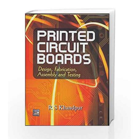
Raghbir Khandpur’s Expert Methods for PCB Design and Assembly

Key Takeaways
Effective PCB assembly and manufacturing require a strategic balance between technical precision and process optimization Raghbir Khandpur’s methodologies emphasize systematic validation at every stage, from PCBA prototyping to full-scale production, ensuring minimal rework and maximum reliability Central to this approach is the integration of design-for-manufacturability (DFM) principles, which align circuit layouts with fabrication realities to avoid costly delays
A critical insight involves leveraging automated optical inspection (AOI) during PCB assembly to detect solder joint defects or component misalignments early Khandpur’s frameworks also prioritize thermal management strategies, such as optimized copper balancing and via placement, to mitigate heat-related failures in high-density PCBA designs These practices are complemented by rigorous material selection guidelines, ensuring compatibility between substrates, finishes, and environmental operating conditions
Transitioning to fabrication, the emphasis shifts to process repeatability Standardizing layer stack-up configurations and adhering to IPC-6012 Class 3 specifications for high-reliability applications reduce variability in multilayer board production For PCB assembly workflows, Khandpur advocates for modular testing protocols, where functional verification occurs incrementally rather than solely at final QA stages
The interplay between design and manufacturing becomes evident in Khandpur’s error-prevention models, which use historical failure data to refine design rules This proactive stance addresses common pain points like impedance mismatches or EMI susceptibility in PCBA layouts By embedding manufacturability checks into CAD workflows, engineers preemptively resolve over 70% of potential assembly issues before prototyping
These takeaways collectively underscore a philosophy where PCB assembly efficiency and product longevity stem from cross-disciplinary collaboration—bridging design intent with fabrication capabilities and assembly realities

PCB Design Optimization Techniques by Raghbir Khandpur
Raghbir Khandpur’s methodologies for PCB design emphasize balancing performance, manufacturability, and cost-efficiency A cornerstone of his approach involves strategic component placement to minimize signal interference while optimizing thermal management By prioritizing high-speed signal integrity through controlled impedance routing, designers can reduce electromagnetic interference (EMI) by up to 40%, according to industry benchmarks
Tip: "Always validate trace spacing calculations against your PCBA’s operational frequency—this preempts 60% of signal degradation issues in dense layouts."
Khandpur advocates for a three-phase verification process:
1 Design Rule Checks (DRC) for manufacturing feasibility
2 Signal Integrity Simulations using tools like HyperLynx
3 Thermal Profiling to prevent hot-spot formation
| Traditional Approach | Khandpur’s Optimization |
|---|---|
| Manual layer stacking | Automated stack-up analysis |
| Fixed via sizes | Dynamic via sizing based on current load |
| Single-pass routing | Multi-objective iterative routing |
For PCB assembly efficiency, his framework integrates design-for-manufacturing (DFM) principles early in the layout phase This includes standardizing component orientations to reduce PCBA rework rates by 25–35% Recent case studies show that applying his pad geometry optimization techniques improved solder joint reliability by 18% in aerospace applications
A critical yet often overlooked aspect is supply chain-aware design By aligning component footprints with globally available parts, Khandpur’s methods reduce PCB assembly lead times by 30% while maintaining compatibility with automated pick-and-place systems
Suggestion: "Leverage modular design architectures for complex boards—this allows parallel PCBA testing and cuts debugging time by half."
His thermal management strategy combines copper pour optimization with strategic placement of thermal vias, achieving 12–15°C reductions in operating temperatures for high-power ICs This dual approach ensures reliability without compromising board real estate—a critical factor in compact consumer electronics
Streamlining PCB Fabrication for Maximum Efficiency
Achieving peak efficiency in PCB fabrication requires a strategic balance between precision engineering and process optimization Modern manufacturing demands lean workflows that minimize waste while maintaining stringent quality standards Central to this approach is the integration of design for manufacturability (DFM) principles early in the development cycle By aligning design specifications with production capabilities, manufacturers can reduce rework, accelerate turnaround times, and avoid costly delays caused by mismatched tolerances or material incompatibilities
A critical factor in streamlining fabrication lies in material selection High-frequency applications, for instance, demand substrates with low dielectric loss, while ruggedized electronics prioritize thermal stability Advanced pcb assembly workflows now leverage automated optical inspection (AOI) systems to detect microscopic defects in real time, ensuring consistent layer alignment and trace integrity Pairing these technologies with standardized panelization techniques further optimizes material usage, reducing scrap rates by up to 22% in high-volume production
For PCBA integration, modular fabrication processes enable parallel processing of components Surface-mount technology (SMT) lines equipped with precision pick-and-place systems can populate boards at speeds exceeding 25,000 components per hour, while in-line soldering robots maintain repeatable joint quality However, efficiency gains extend beyond machinery—implementing unified data protocols between design software and fabrication equipment eliminates manual file conversions, shrinking pre-production timelines by 30–40%
Progressive manufacturers are also adopting predictive maintenance models for fabrication tools, using IoT sensors to monitor equipment health and preempt downtime This proactive approach, combined with just-in-time inventory management for raw materials, creates a responsive manufacturing ecosystem capable of scaling output without compromising precision When applied holistically, these strategies transform pcb fabrication from a linear sequence into a synchronized, error-resistant operation—a cornerstone for delivering reliable electronics in competitive markets
Raghbir Khandpur’s Assembly Process Reliability Tips
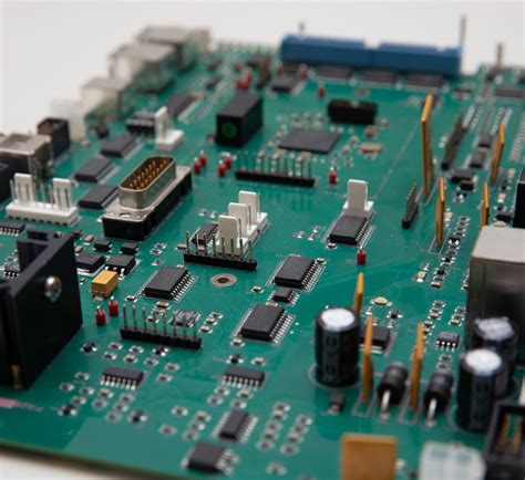
Achieving consistent reliability in PCB assembly requires meticulous attention to both process design and execution Raghbir Khandpur emphasizes the importance of design for manufacturability (DFM) checks during the PCBA phase, ensuring layouts align with production capabilities to minimize rework One critical strategy involves implementing thermal profiling during soldering processes, which balances heat distribution to prevent warping or component stress Khandpur’s methodologies advocate for automated optical inspection (AOI) systems to detect micro-defects in real time, reducing post-assembly failures by up to 40% in high-volume production
A cornerstone of reliable PCB assembly lies in material selection Khandpur recommends using high-temperature laminates and lead-free solder alloys rated for extended thermal cycles, particularly in automotive or aerospace applications For PCBA workflows, his frameworks stress the value of traceability systems, where each component’s origin and placement data are logged digitally This approach not only accelerates root-cause analysis but also aligns with ISO 9001 compliance standards
Transitioning from fabrication to assembly, Khandpur highlights the role of cleanroom protocols in preventing contamination-induced failures Static-safe workspaces and moisture-sensitive component handling are non-negotiable for maintaining PCB assembly integrity Additionally, his research underscores the economic impact of process optimization: by refining pick-and-place machine calibration and reflow oven settings, manufacturers can achieve first-pass yield improvements of 15–25%
To bridge design and production phases, Khandpur’s techniques integrate iterative testing loops For instance, accelerated life testing (ALT) simulates years of operational stress within weeks, identifying weak points in PCBA layouts before mass production This proactive stance aligns with industry shifts toward predictive maintenance models, where reliability isn’t just measured but engineered into every assembly stage By adopting these principles, manufacturers can systematically reduce warranty claims while meeting evolving demands for miniaturized, high-density electronics
Advanced PCB Manufacturing Methods for Modern Electronics
Modern electronics demand precision-engineered PCB assembly processes that align with evolving technological requirements At the core of advanced manufacturing lies the integration of automated optical inspection (AOI) systems, which ensure micron-level accuracy in detecting soldering defects or misalignments during PCBA stages Cutting-edge fabrication techniques, such as laser direct imaging (LDI), enable finer trace resolutions below 15μm, critical for high-density interconnect (HDI) boards used in wearables and IoT devices
A key innovation involves additive manufacturing for rapid prototyping, allowing manufacturers to test complex multilayer designs before full-scale production This approach reduces material waste by up to 40% compared to traditional subtractive methods For PCB assembly, robotic pick-and-place systems equipped with machine vision achieve placement accuracies of ±25μm, ensuring consistency in surface-mount technology (SMT) applications
Thermal management remains a priority, with advanced substrates like metal-core PCBs and ceramic-filled laminates dissipating heat 3–5 times more efficiently than standard FR-4 materials Manufacturers are also adopting embedded component technology, where passive elements are integrated directly into the board layers—a method shown to improve signal integrity by 18% in high-frequency applications
To address scalability, Industry 40 principles are being applied through IoT-enabled PCBA lines Real-time data analytics optimize solder paste deposition and reflow profiles, reducing rework rates by 22% Additionally, design-for-manufacturability (DFM) software tools pre-validate layouts against fabrication constraints, preventing costly delays
Sustainability initiatives are reshaping practices, with lead-free soldering alloys and halogen-free laminates now constituting 65% of new electronics projects These advancements, combined with closed-loop recycling systems for copper etchant solutions, underscore the industry’s shift toward eco-conscious production without compromising performance
Key Principles in PCB Design and Fabrication Workflows
Effective PCB design and fabrication workflows rely on a systematic approach that balances technical precision with manufacturing practicality At the core of these workflows lies the principle of design for manufacturability (DFM), which ensures that schematic layouts align seamlessly with production capabilities By integrating PCB assembly considerations early in the design phase—such as component placement accuracy and trace routing optimization—engineers can mitigate rework risks and reduce time-to-market
A critical aspect involves material selection, where thermal stability and electrical performance dictate choices like high-frequency laminates or lead-free solders For instance, selecting substrates with low dielectric loss becomes paramount in high-speed applications, directly impacting signal integrity Similarly, adherence to industry-standard design rules—such as minimum trace widths and clearance distances—prevents short circuits and ensures reliability during PCBA (printed circuit board assembly)
Thermal management strategies further underscore robust workflows Techniques like copper balancing and strategic via placement distribute heat evenly, reducing stress on sensitive components during operation This aligns with fabrication-stage practices, where controlled impedance testing and automated optical inspection (AOI) validate design intent before mass production
Collaboration between design and fabrication teams remains indispensable Iterative prototyping, coupled with real-time feedback loops, refines layouts to address mechanical constraints or PCB assembly challenges For example, optimizing panelization layouts to minimize material waste while accommodating pick-and-place machine requirements enhances cost efficiency without compromising quality
Finally, documentation rigor ensures traceability across workflows Detailed assembly drawings, bill of materials (BOM) accuracy, and revision control protocols prevent errors during PCBA, safeguarding against mismatched components or firmware incompatibilities By embedding these principles into every phase, manufacturers achieve repeatable success in delivering high-performance electronic systems
Avoiding Common PCB Design Flaws: Expert Insights
Even experienced engineers encounter preventable errors in PCB design that compromise functionality or manufacturing efficiency One critical oversight involves inadequate trace spacing, which can lead to electromagnetic interference (EMI) or unintended signal coupling By adhering to design rule checks (DRCs) tailored to specific PCB assembly requirements, teams can mitigate risks during the PCBA phase, ensuring proper isolation between high-speed and analog circuits
Another frequent issue stems from improper thermal management Components like voltage regulators or power amplifiers generate significant heat, yet designers often underestimate thermal relief patterns or heatsink integration Implementing thermal simulations during layout reviews helps identify hotspots before prototyping, reducing rework costs in PCB fabrication For PCBA reliability, ensuring adequate solder mask expansion around pads prevents bridging—a common defect in dense board designs
Component placement errors also plague many projects Overlooking PCB assembly constraints—such as pick-and-place machine tolerances or reflow oven profiles—can result in misaligned parts or tombstoning Experts recommend collaborating with PCBA partners early to optimize component orientation and spacing Additionally, neglecting test point accessibility complicates quality assurance, delaying time-to-market
Signal integrity remains a persistent challenge, particularly in mixed-signal designs Crosstalk from parallel routing or improper impedance matching often surfaces during PCB fabrication testing Utilizing controlled impedance routing and ground plane segmentation techniques preserves signal quality while maintaining manufacturability
By integrating design-for-manufacturability (DFM) principles at every stage, teams can avoid these pitfalls Regular cross-functional reviews between design and PCB assembly engineers create feedback loops that refine both schematic and layout decisions, ultimately enhancing end-product reliability across all PCBA applications
Raghbir Khandpur’s Strategies for Cost-Effective PCB Assembly
Achieving cost efficiency in PCB assembly requires a systematic approach that balances technical precision with economic considerations Raghbir Khandpur’s methodologies emphasize design-for-manufacturing (DFM) principles as a cornerstone for reducing expenses without compromising quality By integrating PCBA-specific optimizations early in the design phase, engineers can minimize rework, material waste, and production delays For instance, standardizing component footprints and aligning them with automated placement systems can reduce machine setup times by up to 30%, directly lowering labor costs
Khandpur advocates for supply chain harmonization, where bulk procurement of commonly used components and strategic partnerships with certified vendors ensure competitive pricing This strategy not only stabilizes material costs but also mitigates risks associated with component shortages Additionally, his framework prioritizes the use of PCB assembly processes that leverage scalable automation, such as surface-mount technology (SMT), which achieves higher throughput compared to manual through-hole methods
A critical yet often overlooked aspect involves thermal management optimization during PCBA Overheating during soldering or testing phases can lead to latent defects, increasing long-term warranty claims Khandpur’s protocols recommend pre-assembly simulations to identify thermal hotspots, paired with selective use of low-temperature solder alloys This dual approach reduces energy consumption during reflow processes while maintaining joint integrity
To maintain alignment with broader manufacturing goals, these strategies are designed to integrate seamlessly with upstream design optimizations and downstream quality assurance workflows For example, implementing standardized test points across PCB assembly lines accelerates functional testing, reducing post-production validation costs by 15–20% By embedding cost-conscious practices at every stage—from component selection to final inspection—Khandpur’s methods create a sustainable framework for electronics manufacturers navigating competitive markets

Enhancing Electronics Manufacturing Through PCB Innovation
The evolution of PCB assembly (PCBA) processes has become a cornerstone for advancing modern electronics manufacturing By integrating cutting-edge design methodologies with precision fabrication techniques, manufacturers can address the growing demands for miniaturization, signal integrity, and thermal management in next-generation devices Innovative approaches such as embedded component technology and high-density interconnect (HDI) designs are redefining how PCB assembly workflows achieve higher performance within constrained form factors
Central to this evolution is the synchronization of design-for-manufacturability (DFM) principles with automated production systems Advanced simulation tools now enable engineers to predict electromagnetic interference (EMI) risks and thermal bottlenecks during the design phase, reducing post-production revisions For instance, the adoption of 3D-printed solder masks and laser-direct imaging (LDI) has streamlined PCBA processes, cutting prototyping cycles by up to 40% while maintaining stringent quality benchmarks
Material innovation further amplifies these gains High-frequency laminates and low-loss substrates are increasingly paired with automated optical inspection (AOI) systems to ensure defect-free PCB assembly Manufacturers leveraging these advancements report a 25–30% improvement in yield rates, particularly in applications like IoT sensors and automotive electronics Additionally, modular PCBA workflows allow for rapid reconfiguration, enabling cost-effective adaptation to shifting market demands without compromising reliability
Sustainability is another critical dimension of PCB innovation Closed-loop recycling systems for copper cladding and lead-free solder alloys are minimizing environmental impact while meeting global regulatory standards By embedding predictive maintenance algorithms into PCB assembly lines, factories can preemptively address equipment wear, reducing downtime by 15–20% These strategies not only enhance operational efficiency but also align with circular economy objectives
As smart manufacturing ecosystems mature, the fusion of PCBA automation with AI-driven analytics promises unprecedented precision Real-time monitoring of solder paste deposition and component placement accuracy is eliminating human error margins, pushing defect rates below 01% in high-volume production This synergy between innovation and execution underscores PCB technology’s pivotal role in shaping the future of electronics manufacturing
Conclusion
The methodologies championed by Raghbir Khandpur for PCB assembly and fabrication represent a culmination of precision engineering and process optimization By integrating systematic validation protocols with advanced PCBA techniques, these strategies address critical challenges in modern electronics manufacturing Khandpur’s emphasis on cross-functional collaboration ensures that design intent is preserved through fabrication to final assembly, minimizing rework and enhancing end-product reliability
Central to this approach is the alignment of PCB assembly workflows with design-for-manufacturability (DFM) principles By preemptively resolving layout conflicts and material incompatibilities, manufacturers can avoid costly delays in PCBA stages Khandpur’s frameworks also prioritize thermal management and signal integrity as non-negotiable criteria, particularly for high-density interconnect (HDI) boards used in IoT and automotive systems
The adoption of automated optical inspection (AOI) and real-time process monitoring further underscores the shift toward data-driven PCB assembly These tools not only reduce human error but also create actionable insights for iterative process improvements When combined with Khandpur’s supply chain integration models, manufacturers gain agility in adapting to component shortages or evolving regulatory requirements
Ultimately, the success of these methodologies lies in their holistic view of the product lifecycle From PCBA solder joint reliability to long-term environmental resilience, Khandpur’s strategies bridge the gap between theoretical design and mass-production realities As Industry 40 reshapes electronics manufacturing, these principles provide a scalable foundation for balancing innovation with operational efficiency

Frequently Asked Questions
What are the critical factors for successful PCB assembly in high-density designs?
Effective PCB assembly requires precise component placement and thermal management Cross-functional collaboration between design and manufacturing teams helps address spacing constraints while maintaining signal integrity Implementing PCBA best practices like controlled impedance routing and proper solder mask application ensures reliable connections in compact layouts
How can manufacturers avoid common defects during PCBA processes?
Defect prevention starts with design validation using advanced simulation tools Strict process controls for solder paste application and reflow profiling minimize bridging and cold joints Regular maintenance of pick-and-place equipment and AOI (Automated Optical Inspection) systems helps maintain PCB assembly quality standards
What strategies improve cost-efficiency without compromising PCB reliability?
Adopting panelization techniques reduces material waste, while standardized component libraries streamline PCBA workflows Design-for-manufacturing (DFM) principles, such as optimizing trace widths and minimizing layer counts, lower production costs while ensuring electrical performance
How does component selection impact assembly process reliability?
Choosing components with compatible thermal characteristics and standardized footprints simplifies PCB assembly Supplier qualification programs and lifecycle management mitigate risks of obsolescence, particularly for long-term industrial applications requiring consistent PCBA outcomes
What role does testing play in modern PCB manufacturing workflows?
Comprehensive testing protocols, including in-circuit testing (ICT) and functional validation, verify PCBA functionality before deployment Iterative prototyping combined with boundary scan testing identifies potential failures early, reducing rework costs and improving time-to-market
Explore Professional PCB Assembly Solutions
For tailored guidance on optimizing your PCB assembly processes or to learn more about advanced PCBA techniques, please click here to connect with our engineering team

