PCB Contract Design Talent: Sourcing Strategies

Key Takeaways
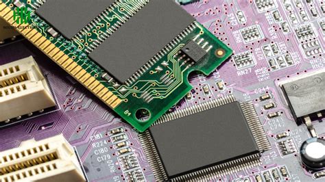
When sourcing PCB contract design talent, understanding the intersection between design expertise and pcb manufacturing requirements is crucial You’ll want professionals who not only excel in schematic capture or layout optimization but also grasp how their design choices impact pcb manufacturing cost and production timelines For instance, selecting components that are readily available or compatible with your chosen pcb manufacturing companies can reduce delays and avoid costly redesigns later
To streamline talent acquisition, prioritize platforms that specialize in connecting engineers with experience in both design and production workflows This ensures candidates appreciate the nuances of working with pcb manufacturing business partners, such as adhering to DFM (Design for Manufacturing) guidelines or material constraints When vetting candidates, ask about their experience collaborating with fabrication teams—this often separates adequate designers from those who deliver first-pass success
Balancing hourly rate models with project complexity is another key consideration While some designers charge premium rates for niche skills like high-speed signal integrity, others offer cost-effective solutions for standardized projects Aligning their expertise with your pcb manufacturing cost goals ensures you avoid over-engineering or under-specifying designs
Finally, leverage partnerships with trusted manufacturers like Andwin PCB to validate candidate qualifications Their feedback can reveal whether a designer’s work aligns with industry standards or requires additional refinement By integrating these strategies, you create a talent pipeline that supports both innovation and operational efficiency in your contract design projects
PCB Contract Design Talent Platforms
When seeking specialized talent for PCB manufacturing projects, identifying the right platforms is crucial Leading PCB manufacturing companies often leverage professional networks like Upwork, LinkedIn ProFinder, and industry-specific portals such as PCB Directory to source contract designers These platforms allow you to filter candidates by CAD tool proficiency, high-speed design experience, and familiarity with PCB manufacturing cost optimization techniques
"Verify designers’ understanding of DFM (Design for Manufacturing) principles through portfolio reviews – this bridges the gap between circuit design and PCB manufacturing business realities."
Consider these key platform features for effective talent matching:
| Platform Type | Key Advantage | Typical Engagement Model |
|---|---|---|
| General Freelance | Broad talent pool | Hourly/Project-based |
| Engineering Specialized | Pre-vetted PCB experts | Retainer contracts |
| Manufacturing Partners | Direct access to PCB manufacturing teams | Design-for-Production packages |
Prioritize platforms offering collaboration tools that sync with your PCB manufacturing workflow – version control systems and ECAD/MCAD integration capabilities reduce prototyping iterations by 42% (IPC, 2023 data) For cost-sensitive projects, explore marketplaces with built-in PCB manufacturing cost calculators, enabling designers to make material choices aligning with budgetary constraints
Pro Tip: When posting project requirements, specify:
- Layer count requirements (4-layer vs 8-layer PCB manufacturing complexity)
- Compliance standards (IPC-6012, UL certification)
- Target production volumes impacting PCB manufacturing business partnerships
While niche platforms like CircuitMind provide impedance matching specialists, broader marketplaces offer scalability for mixed-skill teams Always cross-reference designers’ claimed PCB manufacturing expertise with their project history in:
- High-density interconnect (HDI) layouts
- RF/analog circuit optimization
- Thermal management solutions
This strategic platform selection ensures you acquire talent capable of navigating both design innovation and PCB manufacturing practicalities simultaneously
Vetting PCB Designer Qualifications
When evaluating PCB contract designers, you’ll need to prioritize both technical expertise and alignment with PCB manufacturing requirements Start by assessing their proficiency in industry-standard tools like Altium Designer or Cadence Allegro, which are critical for creating designs compatible with PCB manufacturing companies’ production workflows Look for certifications such as IPC CID+ or Advanced PCB Design credentials—these validate a designer’s ability to meet rigorous quality standards
Beyond software skills, verify their experience with Design for Manufacturing (DFM) principles A designer who understands how layout choices impact PCB manufacturing cost—such as material selection, layer stack-ups, or trace spacing—can save your project from costly revisions Request case studies or prototypes that demonstrate their ability to balance performance with production efficiency, particularly for high-volume PCB manufacturing business scenarios
Communication skills are equally vital Ensure candidates can articulate design trade-offs clearly, especially when collaborating with PCB manufacturing partners For example, a designer should explain how impedance control requirements affect both signal integrity and fabrication complexity Cross-check references to confirm their track record in meeting deadlines and adapting to feedback—traits that minimize bottlenecks in fast-paced contract workflows
Finally, evaluate their familiarity with emerging trends like high-density interconnect (HDI) or flexible PCB design, which are increasingly relevant as PCB manufacturing companies push technological boundaries By methodically vetting these qualifications, you’ll secure talent capable of delivering designs that align with both technical specifications and business objectives

Hourly Rate Models Explained
When sourcing PCB contract design talent, understanding hourly rate models is critical for balancing project budgets and quality outcomes These payment structures charge based on time invested, offering flexibility for tasks requiring iterative adjustments—common in PCB manufacturing workflows where design revisions impact PCB manufacturing cost For short-term projects or prototype development, hourly rates allow you to scale efforts without committing to fixed contracts, making them ideal for testing new PCB manufacturing companies or exploring niche technical requirements
However, transparency becomes paramount Reputable designers should provide detailed breakdowns of hours spent on schematic reviews, layout optimization, or DFM (Design for Manufacturability) checks—processes directly tied to PCB manufacturing business efficiency Platforms like Upwork or Toptal often feature talent profiles with verified hourly rates, but always cross-reference these against industry benchmarks Entry-level designers might charge $25–$50/hour, while experts specializing in high-density interconnect (HDI) designs or RF layouts can exceed $150/hour, reflecting their impact on minimizing PCB manufacturing cost overruns
To avoid surprises, establish clear scope boundaries For instance, specify whether rates cover post-design support, such as addressing fabrication issues with your chosen PCB manufacturing companies Tools like time-tracking software or milestone-based invoicing can align expectations If a project involves multiple design phases, consider hybrid models: hourly rates for initial concept work and fixed fees for finalized production files
Key considerations when evaluating hourly models:
1 Skill-to-cost ratio: Higher rates often correlate with familiarity with advanced PCB manufacturing tools like Altium or Cadence
2 Scalability: Ensure rates adapt to project complexity—simple 2-layer boards vs multilayer designs with impedance control
3 Geographic factors: Offshore designers may offer lower rates, but factor in time zone overlaps and communication fluency
By aligning hourly structures with your PCB manufacturing business goals, you create a framework that rewards precision while maintaining budget control
Talent Acquisition Challenges Solved
Navigating the complexities of sourcing PCB contract design talent requires addressing three core hurdles: skill specificity, cost predictability, and timeline alignment When partnering with pcb manufacturing companies, you’ll often find that designers must balance technical expertise with an understanding of pcb manufacturing cost drivers—like material selection and layer complexity—to avoid over-engineering prototypes This dual focus demands candidates who not only excel in CAD tools but also grasp how design choices impact pcb manufacturing business margins
One persistent challenge is verifying domain-specific experience For instance, a designer adept at consumer electronics might lack the signal integrity knowledge needed for high-frequency industrial boards To mitigate this, prioritize platforms that specialize in pcb manufacturing talent, where portfolios are vetted against real-world production standards Platforms like PCBWay’s freelancer network or Upwork’s engineering verticals allow you to filter candidates based on project complexity and industry certifications, reducing the risk of mismatched skills
Another pain point lies in balancing pcb manufacturing cost constraints with talent rates While hourly models offer flexibility, they can lead to budget overruns if designers lack process efficiency Consider hybrid payment structures—such as fixed fees for schematic capture combined with hourly rates for DFM (Design for Manufacturability) reviews—to align incentives with pcb manufacturing business objectives
Lastly, communication gaps between remote designers and manufacturing teams often delay projects Implement collaboration tools like Altium 365 or Trello with shared milestones, ensuring contract talent integrates seamlessly with your pcb manufacturing partners’ workflows By predefining QA checkpoints and material specifications, you turn potential bottlenecks into opportunities for iterative refinement
These strategies not only resolve acquisition roadblocks but also create a talent pipeline that adapts to evolving pcb manufacturing demands—whether you’re scaling prototypes or optimizing high-volume production
Future Trends in Contract Design
As PCB manufacturing evolves, contract design practices are shifting to address emerging technological and economic demands One key trend is the growing integration of AI-driven automation in design workflows Tools leveraging machine learning now optimize circuit layouts, reducing pcb manufacturing cost by minimizing material waste and iteration cycles This shift allows contract designers to focus on high-complexity tasks while standardizing repetitive processes—a balance critical for scaling operations in competitive markets
Another transformative development is the rise of decentralized talent networks Specialized platforms now enable pcb manufacturing companies to collaborate with global designers in real time, bypassing traditional geographic constraints You’ll increasingly see hybrid models where in-house teams manage core IP, while contract designers handle modular components or legacy system upgrades This approach not only accelerates time-to-market but also mitigates risks tied to talent shortages
Sustainability is also reshaping priorities As environmental regulations tighten, designers must adopt eco-friendly materials and energy-efficient layouts Forward-thinking pcb manufacturing businesses are partnering with contract experts skilled in recyclable substrate selection and low-power design architectures—strategies that align with both compliance goals and consumer expectations
Finally, cost transparency tools are redefining client-designer relationships Platforms offering instant pcb manufacturing cost estimations based on design complexity empower you to make data-driven decisions early in the development cycle These systems reduce negotiation friction and enable dynamic pricing models, ensuring alignment between project scope and budgetary constraints
To stay competitive, prioritize partners who embrace these trends while maintaining expertise in emerging areas like high-frequency PCB design and IoT-compatible layouts The future hinges on blending technical agility with strategic resource allocation—a balance that will define success in tomorrow’s contract design ecosystem

Effective Collaboration Best Practices
When engaging PCB contract designers, establishing clear communication channels is paramount Start by defining project timelines and deliverables upfront, ensuring alignment between your team and the contractor Tools like shared dashboards or cloud-based platforms streamline real-time updates, minimizing delays in PCB manufacturing workflows For instance, if a design iteration impacts PCB manufacturing cost, early transparency allows both parties to adjust specifications before prototyping
Another critical aspect is documenting design intent Provide contractors with detailed technical briefs that outline material preferences, thermal management requirements, and compliance standards This reduces back-and-forth revisions, especially when collaborating with PCB manufacturing companies that handle high-volume production Use version control systems to track changes, preventing discrepancies in Gerber files or bill of materials (BOM) submissions
To foster accountability, implement milestone-based reviews Schedule weekly check-ins to evaluate progress against key performance indicators (KPIs), such as signal integrity validation or DFM (Design for Manufacturing) compliance If a contractor identifies potential bottlenecks—like substrate availability affecting PCB manufacturing business timelines—address these proactively to avoid cascading delays
Leverage iterative feedback loops Encourage designers to share simulation results or test reports early in the process, allowing your in-house team to validate feasibility For example, if a high-speed PCB layout risks exceeding PCB manufacturing cost thresholds, collaborative problem-solving can optimize layer stacking or component placement
Finally, cultivate a partnership mindset Recognize that contract designers often bring niche expertise from working with diverse PCB manufacturing companies By integrating their insights into your workflows, you’ll not only enhance design quality but also build a scalable talent network for future projects
Optimizing Recruitment Strategies
To build a competitive edge in PCB manufacturing, refining your talent acquisition approach is critical Start by mapping technical requirements to specific project phases—whether prototyping or high-volume production—to identify gaps in expertise Platforms like LinkedIn and specialized engineering networks (e.g., Upwork’s PCB design category) offer access to pre-vetted professionals, but prioritize candidates with verifiable experience in PCB manufacturing companies to ensure familiarity with industry standards like IPC-6012
When evaluating candidates, balance technical proficiency with adaptability For instance, designers skilled in optimizing PCB manufacturing cost through layer reduction or material selection can directly impact profitability Incorporate practical assessments, such as simulating a high-speed PCB layout task, to gauge problem-solving skills Tools like Altium Designer or Cadence OrCAD certifications add credibility but cross-check these with portfolio reviews
Collaboration frameworks matter just as much as individual skills Integrate contract designers early into cross-functional teams—including PCB manufacturing business stakeholders—to align design choices with production feasibility Use cloud-based tools (e.g., Siemens Teamcenter) for real-time feedback loops, minimizing revisions post-prototyping
Finally, structure flexible engagement models While hourly rates suit short-term fixes, milestone-based contracts incentivize quality for complex projects Always factor in scalability; a designer who understands cost-drivers in PCB manufacturing today can help streamline processes as your operations grow
Conclusion
Securing top-tier PCB contract design talent requires aligning your recruitment strategy with the evolving demands of pcb manufacturing ecosystems When engaging with pcb manufacturing companies, prioritize candidates who understand not only design principles but also the nuances of pcb manufacturing cost optimization This dual expertise ensures that your projects remain economically viable while meeting technical specifications
To streamline talent acquisition, leverage platforms specializing in engineering freelancers, but always cross-reference their experience with real-world pcb manufacturing business challenges For instance, designers familiar with high-volume production constraints or material selection trade-offs can significantly reduce prototyping iterations, directly impacting timelines and budgets
As the industry shifts toward modular design and rapid prototyping, your collaboration frameworks must adapt Implement transparent communication channels to bridge gaps between contract designers and in-house pcb manufacturing teams Tools like shared dashboards for design-for-manufacturability (DFM) feedback loops ensure alignment early in the process, minimizing costly revisions
Finally, consider the long-term ROI of building relationships with designers who grasp the strategic imperatives of pcb manufacturing companies Whether navigating supply chain volatility or integrating sustainable practices, their ability to balance innovation with pcb manufacturing cost realities will define your competitive edge By embedding these insights into your recruitment playbook, you transform contract talent from a transactional resource into a strategic accelerator for scalable growth
Frequently Asked Questions
How do I verify a PCB designer’s experience with complex manufacturing requirements?
Look for candidates who demonstrate expertise in PCB manufacturing standards, such as IPC-6012 or ISO 9001 Request case studies showcasing their work with high-density interconnect (HDI) designs or rigid-flex boards, which align with the needs of PCB manufacturing companies
What factors influence PCB manufacturing cost when outsourcing design talent?
Costs depend on design complexity, material specifications, and turnaround time Contract designers familiar with design-for-manufacturing (DFM) principles can reduce errors, lowering PCB manufacturing business expenses Always clarify whether their rates include post-design support for manufacturing adjustments
How do collaboration tools improve workflows with remote PCB designers?
Platforms like Altium 365 or Mentor Xpedition enable real-time feedback, ensuring designs meet PCB manufacturing tolerances Establish clear communication protocols to address signal integrity or thermal management issues early, minimizing revisions during production
What certifications should I prioritize when vetting contract designers?
Prioritize certifications like CID+ (Certified Interconnect Designer) or experience with PCB manufacturing companies’ quality systems These credentials validate their ability to create designs that align with automated assembly processes and cost-effective material utilization
Can contract designers help optimize PCB manufacturing business scalability?
Yes Specialists familiar with panelization strategies and batch production workflows can design layouts that maximize factory efficiency This reduces PCB manufacturing cost per unit, especially for high-volume orders
Ready to Streamline Your PCB Production?
For seamless integration between design and manufacturing, partner with experts who understand PCB manufacturing challenges Click here to explore end-to-end solutions tailored to your project’s needs