Why hasn’t AI been applied to PCB drawing?
Applying AI to do layout may not be cheaper than IT labor, and there should be no profit after R&D.
The “scissors gap” between AI R&D investment and income
R&D cost black hole:
Training a usable PCB design AI requires at least 100,000 annotated design drawings (the cost of a single annotation is about 200 yuan), and data preparation alone requires an investment of 20 million yuan. With an annual revenue of over 100 million yuan, there are less than 100 PCB design companies in the world.
Google’s “Circuit Synthesis AI” project cost more than 200 million US dollars, but when it was commercialized, it was found that customers were unwilling to pay a price equivalent to 1.2 times the labor cost.
Obvious ceiling of income:
Assuming that AI increases design efficiency by 50%, under the pricing system of 3 yuan/PIN, the income of a single board will only increase from 3,000 yuan to 4,500 yuan, which cannot cover the computing power cost of AI (such as the hourly usage fee of NVIDIA A100 is about 30 yuan).
The “involution trap” of the industry’s price system makes AI unprofitable
Cost transparency and vicious competition:
The “pricing by PIN” model for PCB design has lasted for many years, which is essentially labor-intensive pricing (for example, 3 yuan/PIN corresponds to an engineer processing 300-800 PIN points per day, the conventional design speed is 300~400Pin/day, which can be accelerated to 400~600Pin/day for free, and the highest speed can reach 800Pin/day (extra expedited fee is required), which is also closely related to the type and complexity of the board). Part-time engineers accept orders at a low price of 1.5-2 yuan/PIN, further squeezing the profit margin.
According to the IPC report, the average price of PCB design services in China is only 1/3 of that in the European and American markets, but the labor cost gap is less than 2 times, and the profit margin is extremely compressed.
Customers generally regard PCB design as “line drawing labor” rather than system engineering with technical content such as electromagnetic compatibility optimization and signal integrity analysis, which makes it difficult to reflect the technical premium in price negotiations.
The design fee of a 6-layer PCB of a motherboard manufacturer has been reduced to 5,000 yuan (about 0.8 yuan/PIN), and engineers need to complete the design + simulation within 3 days, forcing practitioners to rely on templated design rather than technological innovation.
AI’s own answer can only be said to be mediocre. Thinking from a technical perspective:
Although artificial intelligence (AI) has made significant progress in many fields, it still faces some technical and practical challenges in completely replacing manual PCB (printed circuit board) drawing. The following are the main reasons and detailed analysis:
1.Complexity of PCB design
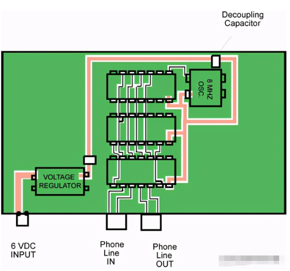
Multidisciplinary integration: PCB design needs to comprehensively consider complex factors such as circuit principles, electromagnetic compatibility (EMC), thermal management, mechanical structure, signal integrity, etc. These constraints are interrelated and require engineers’ domain knowledge and experience to weigh them.
Non-standardized requirements: Different projects have very different requirements for PCB size, number of layers, materials, cost, etc., and it is difficult to cover all scenarios with a single AI model.
Physical and logical coupling: Layout and routing not only need to meet electrical rules, but also need to consider physical limitations such as production processes (such as drilling, welding), heat dissipation paths, etc.
2.Limitations of AI technology
Data scarcity and difficulty in annotation:
PCB design data usually involves corporate secrets, and there are very few public data sets.
Data annotation requires expert knowledge (such as electrical rules and signal priorities), which is costly and time-consuming.
Dynamic optimization and multi-objective trade-offs:
PCB layout needs to optimize multiple goals at the same time (such as minimizing area, reducing signal delay, and enhancing anti-interference). Traditional AI models (such as deep learning) have limited performance in multi-objective dynamic optimization.
Explainability and reliability:
If there are hidden errors (such as signal crosstalk) in the AI-generated solution, it may directly lead to hardware failure. Engineers need to have full controllability and traceability of the design, and black box AI models are difficult to meet this requirement.
3.The degree of automation of existing tools is already high
Auxiliary functions of EDA tools: Modern EDA software (such as Altium Designer and Cadence) have integrated autorouter, DRC (design rule checking) and simulation tools, which greatly improves efficiency.
Exploration of AI-assisted tools:
Some companies have tried to use AI for local optimization (such as high-frequency signal routing and heat dissipation path planning), but the entire process has not yet been covered.
For example, Google used reinforcement learning to optimize the PCB power distribution network, but it was limited to specific modules.
4.Economic and industry inertia
High R&D costs: Developing general PCB design AI requires a lot of resources, and the market return cycle is long, so companies tend to improve existing tools incrementally.
Engineer trust issues: Designers rely more on proven traditional tools and are cautious about the reliability of AI-generated solutions.
Small batch and customized production: Many PCB projects are small batch or customized designs, and AI training data is insufficient, making it difficult to cover long-tail needs.
5.Future development direction
Human-machine collaboration mode: AI may be used to assist engineers in quickly generating candidate solutions (such as layout suggestions and conflict detection) rather than completely replacing manual work.
Breakthrough in subdivided scenarios: In specific areas such as high-density interconnect (HDI) PCBs and RF circuits, AI may be the first to achieve local automation.
Enhanced simulation and verification: Combined with AI to accelerate time-consuming links such as signal integrity simulation and thermal analysis, indirectly improving design efficiency.
Summary
The application of AI in PCB design is still in its early stages, mainly limited by complexity, data barriers and reliability requirements. In the short term, it is more likely to assist engineers in the form of “augmented design” (AI-Augmented Design) rather than completely replace them. With the improvement of reinforcement learning, generative AI (such as Diffusion models) and industry data ecology, more breakthroughs may be seen in the next 5-10 years.