PCB and PCBA: A Comprehensive Guide
Introduction
Printed Circuit Boards (PCBs) and Printed Circuit Board Assemblies (PCBAs) are fundamental components in the electronics industry. PCBs provide the mechanical support and electrical connections for electronic components, while PCBAs are the fully assembled boards ready for use in electronic devices. Understanding the processes involved in PCB fabrication and PCBA assembly is crucial for producing high-quality, reliable, and cost-effective electronic products. This article provides a comprehensive guide to PCB and PCBA, covering various aspects such as design considerations, material selection, fabrication techniques, assembly processes, testing, and quality assurance.
1. PCB Design and Fabrication
1.1 PCB Design
The design phase is the first and most critical step in PCB fabrication. It involves creating a detailed blueprint of the PCB, including the layout of components and the routing of electrical connections. Key considerations during PCB design include:
- Schematic Design: Create a schematic diagram that outlines the electrical connections and components. This serves as the foundation for the PCB layout.
- Component Placement: Place components on the PCB in a way that minimizes trace lengths, reduces noise, and facilitates efficient assembly. Group related components together and consider thermal management for heat-generating components.
- Trace Routing: Route electrical traces to minimize signal interference and ensure proper impedance matching. Use appropriate trace widths and spacing to handle the required current and voltage levels.
- Layer Stackup: Design the layer stackup to optimize signal integrity, power distribution, and thermal management. Use multiple layers if necessary to accommodate complex circuits.
1.2 PCB Fabrication
Once the design is complete, the next step is PCB fabrication. This involves several key processes:
- Substrate Preparation: Start with a substrate material, typically FR-4, which is a glass-reinforced epoxy laminate. The substrate provides the mechanical support for the PCB.
- Copper Cladding: Apply a thin layer of copper to the substrate. This copper layer will be etched to form the electrical traces.
- Photolithography: Use a photoresist and UV light to transfer the PCB design onto the copper-clad substrate. The exposed areas of the photoresist are chemically removed, leaving a pattern that matches the PCB design.
- Etching: Use a chemical solution to etch away the unprotected copper, leaving only the desired traces and pads.
- Drilling: Drill holes for through-hole components and vias. These holes are then plated with copper to create electrical connections between layers.
- Solder Mask Application: Apply a solder mask over the entire PCB, leaving only the pads and vias exposed. The solder mask protects the copper traces from oxidation and prevents solder bridges during assembly.
- Silkscreen Printing: Print component labels, identifiers, and other markings on the PCB using a silkscreen process. This aids in component placement and assembly.

2. PCBA Assembly
2.1 Surface Mount Technology (SMT)
Surface Mount Technology (SMT) is a widely used assembly technique that offers several advantages, including higher component density, improved electrical performance, and cost-effectiveness. The SMT process involves the following steps:
- Solder Paste Application: Apply solder paste to the PCB using a stencil or screen printing process. The solder paste is deposited on the pads where components will be placed.
- Component Placement: Place surface mount components onto the solder paste using a pick-and-place machine. The machine accurately positions each component based on the PCB design.
- Reflow Soldering: Pass the PCB through a reflow oven. The heat melts the solder paste, forming reliable solder joints that electrically and mechanically connect the components to the PCB.
2.2 Through-Hole Technology (THT)
Through-Hole Technology (THT) is used for components that require strong mechanical bonds or high power handling. The THT process involves the following steps:
- Component Insertion: Insert through-hole components into the PCB manually or using an automated insertion machine. The leads of the components pass through holes drilled in the PCB.
- Wave Soldering: Pass the PCB over a wave soldering machine. The machine creates a wave of molten solder that flows over the bottom of the PCB, forming solder joints on the component leads and pads.
2.3 Mixed Technology Assembly
In some cases, a combination of SMT and THT may be required. The mixed technology assembly process involves:
- SMT Assembly: Perform SMT assembly first, including solder paste application, component placement, and reflow soldering.
- THT Assembly: Perform THT assembly next, including component insertion and wave soldering.
3. Testing and Quality Assurance
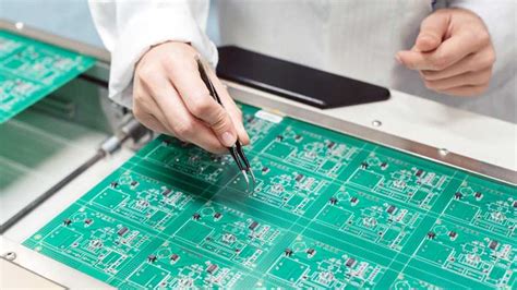
3.1 Automated Optical Inspection (AOI)
Automated Optical Inspection (AOI) is a critical quality control tool in PCBA production. AOI systems use high-resolution cameras and image processing software to detect defects such as soldering issues, missing components, and misaligned parts. By catching defects early, AOI helps reduce rework and scrap costs.
3.2 In-Circuit Testing (ICT)
In-Circuit Testing (ICT) is another essential quality assurance tool. ICT involves using test probes to check the electrical performance of individual components and circuits on the PCB. ICT can quickly identify faults such as open circuits, short circuits, and incorrect component values, ensuring that only high-quality PCBs move to the next stage of production.
3.3 Functional Testing
Functional testing involves testing the assembled PCB to ensure it performs as intended. This type of testing is crucial for verifying that the PCB meets the required specifications and functions correctly in its intended application. Functional testing can be automated to reduce labor costs and improve consistency.
3.4 Environmental Testing
Environmental testing evaluates the PCB’s performance under various environmental conditions, such as temperature extremes, humidity, and vibration. While environmental testing adds to the overall cost, it is essential for ensuring the reliability and durability of the PCB, particularly in demanding applications.
4. Cost-Saving Strategies in PCB and PCBA Production
4.1 Economies of Scale
One of the most effective ways to reduce PCB and PCBA production costs is to take advantage of economies of scale. By increasing production volume, manufacturers can spread fixed costs over a larger number of units, reducing the cost per unit. Strategies to achieve economies of scale include:
- Bulk Production: Produce PCBs in large batches to reduce per-unit costs.
- Long-Term Contracts: Establish long-term contracts with suppliers to secure lower prices for materials and components.
4.2 Outsourcing Assembly
Outsourcing PCB and PCBA production to specialized manufacturers can be a cost-effective strategy, especially for small to medium-sized companies. Benefits of outsourcing include:
- Lower Labor Costs: Outsourcing to regions with lower labor costs can significantly reduce assembly expenses.
- Access to Advanced Technology: Specialized assembly manufacturers often have access to the latest technology and equipment, improving quality and reducing costs.
- Reduced Overhead: Outsourcing eliminates the need for in-house assembly facilities, reducing overhead costs.
4.3 Lean Manufacturing
Implementing lean manufacturing principles can help reduce waste and improve efficiency in PCB and PCBA production. Key lean manufacturing strategies include:
- Just-In-Time (JIT) Production: Produce PCBs only as needed to reduce inventory costs and minimize waste.
- Continuous Improvement: Regularly review and optimize assembly processes to identify and eliminate inefficiencies.
- Quality Control: Implement robust quality control measures to reduce defects and rework, lowering overall costs.
4.4 Design Reuse
Reusing existing PCB designs can save time and reduce development costs. By leveraging proven designs, manufacturers can avoid the costs associated with designing and testing new PCBs. Strategies for design reuse include:
- Modular Design: Develop modular PCB designs that can be easily adapted for different applications.
- Component Standardization: Standardize components across multiple designs to simplify procurement and reduce costs.
- Design Libraries: Maintain a library of proven PCB designs and components for quick reference and reuse.
Conclusion
PCB and PCBA production are complex and multifaceted processes that require careful consideration of design, materials, fabrication techniques, assembly processes, testing, and quality assurance. By optimizing each stage of the production process, manufacturers can achieve high-quality, reliable, and cost-effective electronic products. As the demand for electronic devices continues to grow, mastering the art of PCB and PCBA production will be essential for staying competitive in the market. By following the guidelines outlined in this article, manufacturers can ensure the success of their PCB and PCBA production processes and deliver high-quality electronic products to their customers.