Breaking Down Key Factors in PCB Fabrication Costs
Key Takeaways
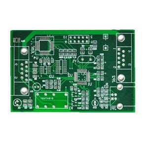
When evaluating pcb manufacturing cost, understanding the primary cost drivers helps you make informed decisions Material selection directly affects expenses—standard FR-4 substrates are cost-effective for most applications, while high-frequency or flexible materials increase pcb manufacturing budgets The number of layers and board dimensions also play pivotal roles: complex multilayer designs require advanced processes, and larger PCB sizes consume more raw materials
PCB manufacturing companies often offer tiered pricing based on order volume—prototypes typically incur higher per-unit costs due to setup fees, while bulk orders benefit from economies of scale Design complexity, such as tight trace spacing or specialized via structures, can escalate expenses by extending production time Faster turnaround times may add premiums, so balancing deadlines with budget constraints is critical
Surface finishes like ENIG or HASL vary in cost, impacting total pcb manufacturing business quotes Testing protocols (e.g., flying probe or AOI) ensure quality but add steps to the workflow Finally, efficient panelization optimizes material usage, reducing waste and lowering per-board costs By prioritizing these factors, you can strategically manage pcb manufacturing cost for both prototypes and large-scale projects

Material Choices in PCB Cost Factors
Your material selection significantly influences PCB manufacturing cost, with substrate type being the primary expense driver Standard FR-4 laminates are cost-effective for general-purpose boards, but specialized applications may require pricier alternatives like high-frequency Rogers materials or flexible polyimide substrates For instance, thermal management needs in LED systems often demand metal-core PCBs (MCPCBs), which increase material costs by 20-30% compared to FR-4
Tip: Work closely with PCB manufacturing companies during the design phase to identify material alternatives that meet performance requirements without over-engineering
Copper weight and dielectric thickness also affect pricing Heavy copper layers (≥3 oz) improve current capacity but raise raw material costs and processing time Similarly, ultra-thin substrates (04mm) require specialized handling, adding 10-15% to baseline PCB manufacturing business expenses When prototyping, consider starting with standard materials and upgrading only after validating electrical performance—this avoids unnecessary costs during early-stage iterations
For high-volume orders, bulk purchasing of specialty materials through established suppliers can reduce per-unit costs Always verify moisture resistance and temperature tolerance specifications, as underperforming materials lead to field failures and hidden expenses Industry benchmarks show that optimizing material choices can lower total fabrication costs by up to 18% without compromising reliability
Layer Count and PCB Size Impact
The number of PCB manufacturing layers directly correlates with production expenses Each additional layer requires more materials, extended processing time, and tighter quality controls, all of which elevate base costs For instance, a 12-layer board may cost 30-50% more than an 8-layer design due to increased copper usage, lamination cycles, and alignment precision PCB manufacturing companies often recommend optimizing layer counts early in the design phase to avoid over-engineering for non-critical applications
Board size is another critical factor Larger PCBs consume more raw materials, but shrinking dimensions too aggressively can raise complexity costs—such as tighter trace spacing or specialized drilling Many PCB manufacturing businesses use panelization to maximize material efficiency, grouping multiple smaller boards onto a single production panel However, oversized designs may limit panel utilization, leading to higher PCB manufacturing cost per unit Balancing size with functional requirements ensures you avoid unnecessary waste while maintaining design integrity
When planning your project, consider how layer count and physical dimensions interact A compact, multilayer design might offer performance benefits but could strain budgets, whereas simpler, larger boards may sacrifice functionality for affordability
Prototype vs Bulk Pricing Models
When evaluating PCB manufacturing costs, understanding pricing structures for prototypes versus bulk orders is critical Prototype production typically incurs higher per-unit expenses due to setup fees, minimum order charges, and lower material utilization rates PCB manufacturing companies often apply premium pricing for small batches to offset these fixed costs, particularly when using advanced processes like HDI or controlled impedance designs
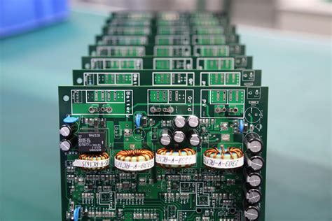
In contrast, bulk manufacturing leverages economies of scale, spreading initial setup and tooling costs across thousands of units This reduces the PCB manufacturing cost per board significantly—often by 40–60% compared to prototypes However, achieving these savings requires careful planning: design finalization, panelization efficiency, and material procurement strategies must be locked in before committing to large volumes
Your choice between prototype and bulk models depends on project stage and risk tolerance While prototypes allow iterative testing, bulk orders optimize long-term PCB manufacturing business budgets Many suppliers offer tiered pricing—negotiate terms that align with your production roadmap, especially if scaling from pilot runs to full-scale manufacturing Balancing these models ensures cost predictability without compromising quality or flexibility
Design Complexity Cost Implications
When working with PCB manufacturing companies, your design choices directly influence PCB manufacturing cost through their impact on production efficiency Trace widths below 015 mm, blind/buried vias, and high-density interconnect (HDI) layouts often require specialized equipment and extended processing times, increasing expenses by 20–40% compared to standard designs For example, a 12-layer board with impedance-controlled routing may cost 25× more than an 8-layer equivalent due to tighter tolerances and additional testing
| Design Feature | Cost Impact | Typical Use Case |
|---|---|---|
| Standard Traces (≥02mm) | Baseline | Consumer Electronics |
| Microvias (≤01mm) | +25–35% | Wearable Devices |
| Flex-Rigid Hybrid | +40–60% | Aerospace Systems |
| Tight Impedance Control (±5%) | +15–25% | High-Speed Networking |
While innovative designs enhance performance, they demand closer collaboration with PCB manufacturing partners to balance technical requirements with PCB manufacturing business realities You’ll want to simplify non-critical areas—reducing via counts or opting for larger solder pads—without compromising functionality Automated design rule checks (DRCs) help identify features that disproportionately escalate costs, such as unnecessary gold plating or oversized silkscreen markings
Transitioning to the next cost driver, remember that even minor design refinements during prototyping can yield substantial savings in production-scale orders
Turnaround Time Cost Trade-Offs
When working with PCB manufacturing companies, you’ll often face a critical balancing act between turnaround time and PCB manufacturing cost Faster production cycles typically come at a premium, as expedited processing requires manufacturers to prioritize your order, adjust production schedules, or allocate overtime labor For instance, a 24-hour prototype service might cost 20–30% more than standard 5–7-day delivery However, slower timelines aren’t always cheaper—delays in bulk orders due to extended lead times could indirectly inflate expenses by delaying product launches
To optimize costs, assess your project’s urgency early If you’re developing prototypes, paying extra for rapid PCB manufacturing might be justified to accelerate testing phases For high-volume PCB manufacturing business orders, plan ahead to leverage standard turnaround windows, avoiding rush fees Some manufacturers offer tiered pricing: economy, standard, and express—each aligning with specific budget and timeline needs
Additionally, batch ordering or aligning production with the manufacturer’s off-peak periods can reduce costs without sacrificing speed Always communicate deadlines clearly; many PCB manufacturing providers will work with you to find a balance between timelines and budget constraints Remember, while faster delivery solves immediate needs, strategic planning often yields the most cost-effective outcomes

Surface Finish Cost Variations
Your choice of PCB manufacturing surface finish directly impacts both performance and budget Common options like HASL (Hot Air Solder Leveling), ENIG (Electroless Nickel Immersion Gold), and Immersion Silver vary significantly in PCB manufacturing cost, with basic finishes costing 5–10% of the total board price, while premium options can exceed 15% For instance, ENIG offers superior flatness and shelf life but adds 20–30% more expense compared to HASL—a trade-off PCB manufacturing companies often weigh against application requirements like high-frequency signal integrity or corrosion resistance
When prototyping, you might prioritize cost-effective finishes to minimize upfront expenses However, bulk orders benefit from negotiating volume discounts on advanced coatings, especially if your PCB manufacturing business involves industrial-grade products requiring durable finishes Emerging alternatives like OSP (Organic Solderability Preservative) provide mid-range pricing but require tighter process control, illustrating how technical constraints influence financial decisions Always align your finish selection with both functional needs and long-term reliability goals—overspending on unnecessary specs or underspending on critical protections can erode profitability in later stages
Testing Impact on PCB Expenses
When evaluating PCB manufacturing cost, testing protocols often represent a hidden variable that significantly influences your final expenses While skipping tests might reduce upfront costs, it risks undetected defects that lead to costly rework or field failures Most PCB manufacturing companies implement electrical testing (e.g., flying probe or fixture-based) to verify circuit continuity, but advanced methods like automated optical inspection (AOI) or boundary scan testing add layers of precision—and cost—depending on your design’s complexity
For prototypes, you might opt for basic testing to validate functionality without overspending However, in bulk orders, comprehensive testing becomes critical to maintain quality across thousands of units Striking a balance here depends on your product’s application: high-reliability industries (medical, aerospace) demand rigorous testing, while consumer electronics may tolerate leaner protocols
Your PCB manufacturing business partners can often tailor testing packages, but remember: tighter tolerances and higher layer counts inherently require more sophisticated—and expensive—validation Always clarify testing requirements early in the design phase to avoid budget overruns, as retrofitting tests mid-production inflates costs disproportionately
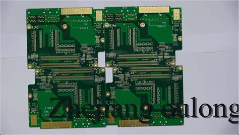
Panelization for Cost Efficiency
Effective panelization strategies directly influence PCB manufacturing costs by optimizing material usage and production efficiency When you design multiple smaller boards into a single panel, PCB manufacturing companies can reduce material waste and streamline processes like drilling, plating, and routing This approach is particularly impactful for high-volume orders, where maximizing the number of boards per panel lowers the cost per unit significantly However, improper panelization—such as inefficient spacing or irregular board shapes—can increase scrap rates and negate potential savings
A critical balance lies in aligning panel designs with fabrication capabilities For instance, standard panel sizes (e.g., 18" x 24") minimize setup adjustments, while intelligent array layouts reduce tooling time Additionally, incorporating breakaway tabs or V-scoring ensures easier depaneling without damaging individual boards, avoiding post-production rework costs Collaborating with your PCB manufacturing business partner early in the design phase helps identify optimal panel configurations tailored to your project’s complexity and volume
Remember: while panelization cuts PCB manufacturing cost, over-optimization might compromise quality Tightly packed panels could lead to handling challenges or solder mask inconsistencies Always prioritize manufacturability alongside cost-saving measures to maintain reliability
Conclusion
Navigating PCB manufacturing costs requires balancing technical requirements with budget constraints When partnering with PCB manufacturing companies, you’ll find that costs are shaped by interconnected variables—from material specifications to design iterations While PCB manufacturing business models often prioritize bulk orders for economies of scale, even low-volume prototype runs can stay cost-effective through smart panelization and standardized testing protocols
To optimize PCB manufacturing cost, always align your design choices with production realities Simplify layouts where possible, select surface finishes that match functional needs, and leverage volume discounts without overordering Remember that faster turnaround times may inflate expenses, so plan timelines strategically By fostering open communication with manufacturers and refining designs iteratively, you’ll build a framework for balancing quality, speed, and affordability across projects
Frequently Asked Questions (FAQs)
How does material selection affect pcb manufacturing cost?
Material choices directly influence expenses—high-frequency laminates or specialized substrates cost more than standard FR-4 PCB manufacturing companies often provide tiered pricing based on material grades, balancing performance needs with budget constraints
Why do bulk orders reduce pcb manufacturing expenses?
Economies of scale apply: higher order volumes spread setup costs (like tooling) across more units For pcb manufacturing business clients, bulk pricing models typically offer discounts of 15-40% compared to prototype runs
Can design complexity impact turnaround timelines?
Yes Intricate designs with tight tolerances or high-density interconnects require advanced processes, extending production time Faster turnaround options may incur 20-30% premiums, depending on the pcb manufacturing provider’s capabilities
How does panelization optimize costs?
Efficient panel layouts minimize material waste Many pcb manufacturing companies use software to nest multiple boards per panel, reducing per-unit costs by 5-15% while maintaining quality standards
Are testing fees included in base pcb manufacturing cost?
Basic electrical testing is often bundled, but specialized checks (e.g., impedance validation or X-ray inspection) add 8-20% to total costs Always clarify testing scope with your supplier
Need a Custom Quote for Your Project?
For tailored solutions that align with your pcb manufacturing budget and technical requirements, please click here to connect with industry experts