Precision Circuit Board Assembly Services for Advanced Applications
Key Takeaways
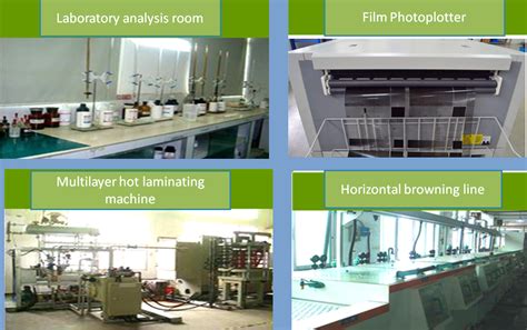
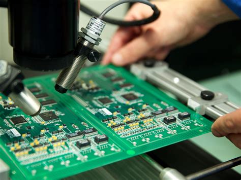
Modern PCB assembly services form the backbone of mission-critical industries, combining precision engineering with rigorous quality frameworks. From aerospace avionics to implantable medical devices, PCBA providers leverage advanced SMT technology to achieve micron-level accuracy, ensuring compliance with ISO 13485 (medical) and AS9100D (aerospace) standards. Industrial-grade solutions prioritize thermal resilience and vibration resistance, particularly for energy infrastructure and automation systems operating in extreme environments.
Tip: When evaluating circuit board assembly companies, verify their traceability protocols for materials and automated optical inspection (AOI) coverage—critical for applications where component failure carries catastrophic risks.
Leading providers now integrate high-density interconnect (HDI) designs with embedded component PCBA, enabling 30%+ size reduction for compact industrial sensors and diagnostic equipment. Real-time process monitoring during PCB assembly minimizes microvoids in solder joints, a vital enhancement for satellite communications hardware. For harsh-environment deployments, conformal coating services and MIL-STD-883G testing ensure PCBA longevity in high-humidity or chemically aggressive settings.
Precision PCB Assembly for Aerospace Systems
Aerospace systems demand PCB assembly processes that meet exceptionally rigorous performance and reliability standards. Modern PCBA for avionics, satellite communications, and flight control systems requires adherence to MIL-PRF-31032 and IPC-A-610 Class 3 specifications, ensuring resistance to extreme temperatures, vibration, and electromagnetic interference. Leading manufacturers employ advanced SMT (surface-mount technology) to achieve component placement accuracy within ±25μm, critical for high-density layouts in compact aerospace electronics.
| Key Aerospace PCB Requirements | Technical Specifications |
|---|---|
| Operating Temperature Range | -55°C to +125°C |
| Vibration Resistance | 20–2000 Hz, 15G peak |
| Signal Integrity Standards | IPC-6012EM Class 3A |
| Mean Time Between Failures | >500,000 hours |
To ensure zero-defect outcomes, PCB assembly partners utilize automated optical inspection (AOI) and X-ray testing to detect micro-cracks or solder voids invisible to the naked eye. Conformal coating applications with MIL-I-46058-certified materials further protect boards from moisture and chemical exposure in stratospheric environments. As aerospace applications increasingly integrate AI-driven subsystems, PCBA providers are adopting laser-direct imaging (LDI) for sub-20μm trace widths, enabling faster signal processing in next-gen navigation systems. This precision aligns with the industry’s shift toward miniaturized, weight-optimized designs without compromising functional redundancy.
Collaboration with PCB assembly specialists certified in AS9100D ensures compliance with aviation-specific traceability protocols, from component sourcing to final system integration.

Advanced SMT Solutions for Medical Devices
Modern medical devices demand unparalleled precision in PCB assembly (PCBA) to ensure reliability in life-critical applications. Surface-mount technology (SMT) has evolved to meet these stringent requirements, enabling the integration of micro-components like 0.4mm-pitch BGAs and 01005 passives onto high-density interconnect (HDI) boards. Leading circuit board assembly companies leverage automated optical inspection (AOI) and X-ray systems to verify solder joint integrity, particularly for implantable devices where failure is not an option.
The shift toward flexible hybrid electronics (FHE) in wearable medical monitors underscores the need for advanced SMT processes that accommodate stretchable substrates without compromising signal fidelity. For surgical robotics and imaging systems, low-temperature co-fired ceramic (LTCC) substrates paired with PCBA workflows ensure thermal stability during repeated sterilization cycles.
Quality protocols exceed standard ISO 13485 certifications, incorporating traceability blockchains for component-level accountability—a non-negotiable feature in FDA-regulated environments. As miniaturization accelerates, PCB assembly specialists now deploy nano-coating technologies to protect circuitry from bodily fluids in diagnostic patches and smart drug delivery systems. This convergence of precision manufacturing and regulatory rigor positions SMT as the backbone of next-generation medical innovation.
Industrial-Grade Circuit Board Manufacturing
Industrial applications demand PCB assembly solutions that withstand extreme operational conditions while maintaining consistent performance. Unlike consumer electronics, industrial-grade PCBA requires robust material selection, including high-temperature laminates and copper substrates, to ensure durability in environments with vibration, humidity, or temperature fluctuations. Manufacturers specializing in this sector prioritize design-for-manufacturability principles, balancing component density with thermal management to prevent overheating in enclosed systems like motor controllers or automation equipment.
Advanced SMT assembly techniques, combined with through-hole technology for larger components, create hybrid boards capable of handling high-power loads common in industrial robotics and machinery. Rigorous quality assurance protocols, such as automated optical inspection (AOI) and thermal cycling tests, verify board integrity before deployment. Leading circuit board assembly companies also implement conformal coating processes to protect against chemical exposure in manufacturing plants or outdoor installations.
These specialized PCBA services support applications ranging from programmable logic controllers to IoT-enabled sensors, where failure tolerance approaches zero. By integrating redundancy features and fail-safe circuitry, industrial-grade manufacturers ensure uninterrupted operation in mission-critical infrastructure, aligning with global standards like IPC-A-610 Class 3 for harsh environment electronics.
Quality Control in Mission-Critical Electronics
In mission-critical sectors such as aerospace, medical technology, and industrial automation, PCB assembly processes demand uncompromising quality control protocols. Leading PCBA providers implement multi-layered inspection systems, combining automated optical inspection (AOI) with X-ray analysis to detect microscopic defects in solder joints, component alignment, and substrate integrity. For high-reliability applications, traceability is paramount — every resistor, IC, and connector is logged through barcode or RFID systems to ensure full compliance with ISO 9001:2015 and IPC-A-610 Class 3 standards.
Advanced PCB assembly workflows integrate environmental stress testing (EST), exposing boards to thermal cycling, vibration simulations, and humidity chambers that replicate end-use conditions. Statistical process control (SPC) tools monitor production data in real time, flagging deviations as small as 0.2% in solder paste deposition volumes. This meticulous approach reduces failure rates to below 15 parts per million (PPM) in defense and medical PCBA projects.
To maintain consistency, certified manufacturers employ closed-loop corrective action systems, where test failures trigger root-cause analyses and process refinements within 24 hours. Such rigor ensures that mission-critical electronics meet zero-defect thresholds while adhering to stringent MIL-PRF-31032 and NASA-STD-8739.4 specifications for long-term operational reliability.
Innovations in High-Density PCB Assembly
Modern PCB assembly processes are undergoing transformative advancements to meet the demands of miniaturized electronics and ultra-compact designs. Leading PCBA providers now leverage laser-drilled microvias and advanced stacked via configurations to achieve interconnection densities exceeding 150,000 traces per square inch. These innovations enable multilayer boards with embedded passive components, reducing footprint while enhancing signal integrity in aerospace avionics and medical imaging systems.
The integration of 3D printing technologies for hybrid substrates allows PCB assembly firms to embed sensors and RF modules directly into rigid-flex designs, critical for IoT-enabled industrial equipment. Additionally, automated optical inspection (AOI) systems paired with AI-driven defect detection ensure sub-20μm alignment accuracy, a necessity for high-density PCBA in satellite communications and robotics.
To address thermal management challenges, cutting-edge liquid-cooled interposers and ceramic-filled laminates are being adopted, extending component lifespans in harsh environments. These advancements position PCB assembly as a cornerstone for next-gen applications, balancing high-speed performance with structural resilience across mission-critical sectors.
Choosing Reliable Circuit Board Assembly Partners
Selecting PCB assembly partners requires balancing technical expertise with proven operational rigor. Mission-critical sectors like aerospace and medical device manufacturing demand partners with PCBA capabilities that align with stringent regulatory frameworks. Key indicators include certifications (e.g., ISO 9001, IPC-A-610), advanced SMT assembly infrastructure, and traceability systems for component-level accountability.
Equally important is evaluating a vendor’s adaptability to high-mix, low-volume production scenarios common in industrial tech. Partners should demonstrate proficiency in high-density PCB assembly, including microvia drilling and fine-pitch component placement, while maintaining zero-defect thresholds for solder joints and electrical continuity.
This requires transparent communication channels for design-for-manufacturability (DFM) feedback, particularly when scaling prototypes to full production. Supply chain resilience also plays a pivotal role—verified through audits of component sourcing practices and contingency planning for obsolescence management.
Moreover, prioritize PCB assembly providers offering comprehensive testing protocols, such as automated optical inspection (AOI) and in-circuit testing (ICT), to mitigate risks in harsh-environment applications. A partner’s ability to integrate IoT-enabled process monitoring often correlates with reduced time-to-market and lifecycle cost efficiencies.
Ultimately, the right PCBA collaborator becomes an extension of your engineering team, ensuring seamless alignment between design intent and manufacturable outcomes.
SMT Technology for Harsh Environment Applications
In demanding industrial settings where temperature extremes, moisture, or vibration threaten electronic reliability, specialized PCB assembly processes must integrate robust SMT (Surface Mount Technology) solutions. Advanced automated optical inspection systems and high-temperature soldering alloys enable PCBA providers to create assemblies capable of enduring harsh operational conditions. For applications such as offshore energy systems or military communications, manufacturers employ conformal coatings and hermetic sealing techniques to protect components from corrosive elements while maintaining signal integrity.
Modern PCBA workflows leverage vibration-resistant mounting patterns and thermal management substrates to mitigate mechanical stress and heat accumulation. Rigorous environmental stress screening (ESS) protocols validate performance under simulated extreme conditions, ensuring compliance with MIL-STD-810 or IP68 standards. By combining precision PCB assembly with materials engineered for durability, manufacturers deliver mission-ready electronics that maintain functionality in -40°C Arctic deployments or 150°C industrial furnace environments. This technological synergy supports seamless integration with subsequent PCB testing protocols, forming a cohesive quality assurance chain for critical infrastructure systems.
PCB Testing Protocols for Industrial Tech
Industrial technology applications demand PCB assembly solutions that withstand extreme operational conditions, from temperature fluctuations to mechanical stress. Rigorous testing protocols ensure PCBA reliability, combining automated optical inspection (AOI), in-circuit testing (ICT), and functional validation. For mission-critical systems, thermal cycling tests simulate extended exposure to temperature extremes, while vibration testing replicates real-world mechanical wear.
Leading circuit board assembly companies employ boundary-scan techniques to verify complex circuitry, particularly for high-density interconnects common in industrial automation. Environmental stress screening (ESS) further identifies latent defects by subjecting boards to accelerated aging processes. These protocols align with IPC-A-610 and ISO 9001 standards, ensuring PCB assembly outcomes meet industrial-grade durability requirements.
Advanced PCBA providers integrate predictive analytics into test workflows, leveraging machine learning to identify failure patterns in multilayer boards. This data-driven approach optimizes testing efficiency while maintaining zero-defect thresholds for safety-critical applications. Transitioning to these protocols enables manufacturers to address evolving industrial demands, from smart grid controllers to robotic systems, without compromising production scalability.
Conclusion
Selecting the right PCB assembly partner remains pivotal for industries requiring mission-critical electronic systems. As aerospace, medical, and industrial technologies advance, the demand for PCBA solutions that balance precision, durability, and innovation continues to escalate. Leading manufacturers distinguish themselves through cutting-edge SMT processes, rigorous testing protocols, and adherence to aerospace-grade certifications, ensuring reliability even in extreme operating conditions.
When evaluating circuit board assembly companies, prioritize those offering end-to-end traceability and specialized expertise in high-density interconnect (HDI) or flexible PCB designs. The integration of automated optical inspection (AOI) and X-ray testing underscores a commitment to zero-defect manufacturing, a non-negotiable standard for sectors like avionics or implantable medical devices.
Ultimately, the convergence of PCB assembly excellence with domain-specific engineering knowledge enables the production of systems that meet next-generation performance thresholds. As industries push the boundaries of miniaturization and thermal resilience, partnering with PCBA providers that invest in R&D and scalable production methodologies will remain central to achieving long-term technological success.
FAQs
What certifications should I look for in a high-reliability PCB assembly partner?
Reputable PCBA providers typically hold ISO 9001, AS9100 (for aerospace), and ISO 13485 (for medical devices). These certifications validate adherence to rigorous quality management systems, essential for PCB assembly in mission-critical sectors.
How do harsh-environment applications impact material selection for circuit boards?
Industrial and aerospace systems require substrates like polyimide or ceramic-based laminates to withstand extreme temperatures and vibrations. Trusted PCB assembly companies pair these materials with conformal coating and advanced SMT assembly techniques to ensure long-term durability.
What testing protocols ensure reliability in medical-grade PCBAs?
Beyond standard AOI and ICT, medical PCBA services employ HALT/HASS testing to simulate decades of operational stress. Biocompatibility validation is also critical for devices interfacing with human tissues.
Can high-density designs compromise manufacturability?
While 0.3mm microvias and 01005 components enable miniaturization, they demand precision PCB assembly workflows. Leading partners use 3D SPI and X-ray inspection to maintain yield rates above 99.95% in HDI projects.
Why do aerospace PCBAs require extended lead times?
Compliance with MIL-PRF-31032 and NASA-STD-8739 standards involves exhaustive documentation and lot-traceability protocols. For radiation-hardened satellite electronics, additional thermal cycling tests add 2-3 weeks to production schedules.
Explore Custom PCB Assembly Solutions for Your Project
For tailored PCB assembly strategies meeting industry-specific requirements, please click here to consult with engineers specializing in aerospace, medical, and industrial PCBA challenges.