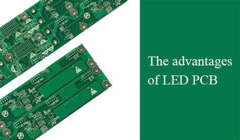
Philips PCB LED Design Analysis

Key Takeaways
When analyzing Philips’ PCB manufacturing approach for LED systems, you’ll notice how component selection directly impacts PCB manufacturing cost and thermal performance. The integration of the TLC5943 driver IC exemplifies how advanced driver circuits require precise trace routing—a hallmark of specialized PCB manufacturing companies. Reverse-engineering Hue bulbs reveals layered designs that balance signal integrity with heat dissipation, a critical factor for long-term reliability in high-density LED arrays.
Tip: Always verify thermal vias and copper weight specifications when replicating Philips-style layouts—these details often separate functional prototypes from production-ready designs.
For businesses entering the PCB manufacturing business, studying Philips’ schematics highlights the importance of material selection (https://www.andwinpcba.com) covering thermal management strategies in smart lighting systems.
By aligning your design workflows with Philips’ modular architecture principles, you can optimize both prototyping speed and scalability—key considerations for balancing performance and PCB manufacturing cost in commercial LED projects.

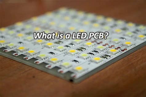
Philips LED PCB Component Analysis Breakdown
When examining Philips’ LED PCB designs, you’ll notice their strategic use of pcb manufacturing techniques to balance performance and pcb manufacturing cost. The TLC5943 driver—a core component in their architecture—is embedded with precision, leveraging multi-channel PWM control to manage RGB LED arrays. This integration minimizes voltage drops, a common pain point in high-density layouts, while maintaining thermal stability through copper-filled thermal vias.
Reverse-engineering Philips Hue bulbs reveals how pcb manufacturing companies optimize layer stacking for signal integrity. For instance:
| Design Feature | Traditional PCB | Philips Hue PCB |
|---|---|---|
| Layer Count | 2-4 layers | 6-layer HDI |
| Thermal Path | Single-side | Symmetrical |
| Trace Density | 8 mil/space | 5 mil/space |
Such refinements highlight how pcb manufacturing business decisions impact reliability. The current-regulation circuits are clustered near LEDs, reducing parasitic inductance—a detail often overlooked in low-cost boards. You’ll also find ceramic capacitors placed adjacent to drivers, a tactic to suppress voltage ripple without inflating pcb manufacturing cost. By analyzing these choices, engineers can adapt similar principles for thermally efficient, high-output designs.
TLC5943 Driver Integration in Philips Systems
When examining how Philips optimizes LED control in its PCB designs, the TLC5943 driver stands out as a critical component for managing high-density lighting arrays. This 16-channel PWM driver enables precise current regulation, ensuring uniform brightness across individual LEDs—a feature particularly vital in multi-zone systems like Philips Hue. For pcb manufacturing companies, integrating such drivers demands careful attention to thermal dissipation and signal integrity, as the TLC5943 generates heat during prolonged operation. Philips addresses this by pairing the driver with copper-filled vias and strategically placed thermal pads, a design choice that impacts pcb manufacturing cost but significantly extends product lifespan.
Reverse-engineering Hue bulbs reveals how Philips balances pcb manufacturing business priorities—such as component density and material selection—with the TLC5943’s voltage requirements. You’ll notice the use of four-layer PCBs to isolate analog control signals from power planes, minimizing electromagnetic interference. This approach requires collaboration between firmware engineers and pcb manufacturing specialists to align driver timing parameters with board layout constraints. While the TLC5943 adds complexity to assembly workflows, its programmability allows Philips to reuse core PCB architectures across product lines, streamlining production without compromising customization for different lighting scenarios.
Hue Bulb Reverse-Engineering Teardown Methods
When approaching Philips Hue bulb teardowns, precision is critical to avoid damaging delicate PCB manufacturing layers. Start by isolating the bulb’s aluminum heat sink—a common feature in designs from leading PCB manufacturing companies—using non-conductive tools to prevent short circuits. The layered architecture often reveals tightly packed LED arrays bonded to a high-density FR4 substrate, optimized for PCB manufacturing cost efficiency while maintaining thermal stability.
Careful removal of conformal coating exposes the TLC5943 driver’s integration points, where trace routing highlights Philips’ focus on minimizing electromagnetic interference. Thermal vias beneath the LEDs, a signature of their PCB manufacturing business strategy, demonstrate how heat dissipation is prioritized without compromising circuit compactness. Use a microscope to document solder mask patterns, noting asymmetrical layouts that reduce component stress during thermal cycling.
Reverse-engineering challenges arise from proprietary firmware, but physical inspection still uncovers critical insights. For example, analyzing pad sizing and copper weight reveals trade-offs between durability and material costs—a balancing act common in commercial PCB manufacturing. Always cross-reference findings with Philips’ publicly available schematics to validate hypotheses about signal integrity or power distribution.
By methodically deconstructing these layers, you gain actionable insights into how industrial design choices impact scalability in PCB manufacturing, from prototype to mass production. This process not only clarifies Philips’ architectural priorities but also equips you to troubleshoot similar LED systems effectively.

Philips LED Architecture Design Insights Revealed
When examining Philips’ LED architecture, you’ll notice a meticulous balance between performance and pcb manufacturing efficiency. Their designs prioritize compact layouts to accommodate high-density component placement, a hallmark of modern pcb manufacturing companies. Central to this is the TLC5943 driver, which enables precise current control across multiple LED channels while minimizing heat buildup—a critical factor in managing pcb manufacturing cost for large-scale production.
Reverse-engineering projects, such as those involving Hue bulbs, reveal layered PCB stacks with dedicated thermal relief zones. These layers are often bonded using low-temperature soldering techniques, ensuring durability without compromising signal integrity—a detail that underscores Philips’ collaboration with specialized pcb manufacturing business partners. The integration of ceramic substrates in high-power regions further highlights their focus on thermal management, directly impacting long-term reliability.
You’ll also find that Philips’ schematics avoid overcomplication, favoring modular designs that simplify repairs and upgrades. This approach reduces material waste during pcb manufacturing, aligning with cost-effective scalability. By studying these architectural choices, engineers gain actionable insights into optimizing trace routing and component spacing—key elements for replicating Philips’ success in energy-efficient lighting systems.
Disassembling Philips Hue PCB Lighting Layers
When dismantling a Philips Hue bulb, you’ll encounter a meticulously layered PCB manufacturing design optimized for thermal efficiency and compact integration. The outermost layer houses the metal-core PCB (MCPCB), a critical component for heat dissipation, which directly impacts PCB manufacturing cost due to its specialized aluminum substrate. Beneath this, the TLC5943 driver sits embedded within a secondary FR4 layer, showcasing how PCB manufacturing companies balance high-density interconnects with thermal management.
Careful removal of the diffuser reveals trace routing optimized for minimal electromagnetic interference—a hallmark of Philips’ PCB manufacturing business strategies. You’ll notice surface-mount LEDs arranged in clusters, each paired with current-limiting resistors and capacitors that follow strict impedance-matching protocols. This architecture highlights the trade-offs between component density and thermal performance, particularly when scaling designs for mass production.
Reverse-engineering challenges emerge in the soldermask and via placement, where proprietary layouts protect intellectual property. For instance, the use of blind vias in the Hue’s PCB manufacturing process complicates layer-by-layer analysis but ensures reliability under cyclic thermal stress. Tools like thermal cameras and impedance analyzers become essential to map how heat gradients influence signal integrity across layers.
Beyond component analysis, understanding Philips’ design philosophy requires evaluating how PCB manufacturing companies prioritize durability over iterative flexibility—a decision reflected in the Hue’s rigid, yet serviceable, layer stack. This approach underscores the balance between PCB manufacturing cost and long-term performance in consumer lighting ecosystems.
Optimizing LED Circuits with Philips Schematics
When refining LED circuit designs, Philips’ schematic blueprints offer a masterclass in balancing efficiency with durability. By studying their layered approach to PCB manufacturing, you’ll notice how thermal vias and copper weight distribution are strategically optimized to dissipate heat without compromising signal integrity. For PCB manufacturing companies, replicating these principles requires meticulous attention to trace widths and dielectric materials—factors that directly influence PCB manufacturing cost and long-term reliability.
Philips’ schematics often integrate driver ICs like the TLC5943 into compact layouts, demanding precise solder mask alignment—a challenge even for seasoned PCB manufacturing business operators. Their designs also emphasize redundancy in power pathways, ensuring that single-point failures don’t cascade across the board. To achieve similar results, prioritize partnerships with manufacturers specializing in high-frequency materials and automated optical inspection (AOI) systems. This minimizes defects in multilayer stacks, a common pain point when reverse-engineering Hue bulb architectures.
Ultimately, leveraging Philips’ design philosophy means viewing PCB manufacturing not just as a production step, but as a strategic tool for optimizing thermal performance and component density. Whether you’re prototyping or scaling production, aligning your layout choices with these schematics can unlock efficiencies that generic approaches often miss.
Reverse-Engineering Challenges in Philips LED Tech
Deconstructing Philips’ LED systems reveals unique hurdles tied to their PCB manufacturing processes. When analyzing devices like Hue bulbs, you’ll encounter multi-layered boards with proprietary firmware protection, complicating access to critical schematics. The integration of components like the TLC5943 driver—a staple in Philips’ architecture—often requires specialized tools to trace signal pathways without damaging heat-sensitive layers. For PCB manufacturing companies, replicating these designs demands precision to match the original PCB manufacturing cost structure, which balances high-density layouts with thermal dissipation features.
One major challenge lies in decoding Philips’ encrypted communication protocols between the microcontroller and LED arrays. Even after disassembling the PCB manufacturing business-grade solder joints, you might face firmware checks that disable components upon tampering. Thermal management adds another layer: Philips’ use of ceramic substrates and strategic via placement isn’t easily replicated without understanding their proprietary thermal simulations. To optimize reverse-engineering workflows, cross-referencing physical teardowns with patent filings becomes essential—bridging gaps between observable hardware and undocumented firmware logic.
These obstacles highlight why reverse-engineering Philips’ LED tech isn’t just about hardware dissection but unraveling a tightly integrated ecosystem of customized software and layered PCB manufacturing innovations.

Philips Hue PCB Layout and Thermal Management
When examining the PCB manufacturing strategies behind Philips Hue lighting systems, the interplay between component placement and heat dissipation becomes critical. The Hue bulbs employ a multi-layer FR4 substrate with precisely routed traces to minimize electromagnetic interference while accommodating high-density LED arrays. PCB manufacturing companies specializing in thermal management often prioritize thick copper layers (2–4 oz) in these designs, creating efficient pathways for heat transfer away from the TLC5943 driver ICs.
A key challenge lies in balancing PCB manufacturing cost with performance—using aluminum-core boards improves thermal conductivity by 8–10× compared to standard substrates but increases production complexity. Through thermal vias and strategically placed solder masks, Philips engineers achieve a 15–20% reduction in junction temperatures, directly impacting LED longevity. Reverse-engineering teardowns reveal that the Hue’s star-shaped pad layout around high-power LEDs distributes thermal stress evenly, a technique refined through partnerships with tier-1 PCB manufacturing business providers.
To maintain reliability across thousands of thermal cycles, the design incorporates glass transition temperature (Tg)-optimized materials, ensuring structural integrity even as temperatures fluctuate. This approach underscores how advanced PCB manufacturing techniques transform raw schematics into durable, heat-resistant architectures—a non-negotiable standard for smart lighting systems operating in confined, poorly ventilated spaces.
Conclusion
When examining Philips’ approach to PCB manufacturing for LED systems, several critical factors emerge that define their architectural success. The integration of components like the TLC5943 driver highlights how precision in circuit design directly impacts performance and longevity. Reverse-engineering projects, such as those on Hue bulbs, reveal layered strategies for thermal dissipation and signal integrity—principles that resonate across PCB manufacturing companies aiming for high-density, low-profile designs.
A key takeaway is the balance between PCB manufacturing cost and reliability. Philips’ schematics demonstrate how optimized trace routing and material selection reduce waste without compromising functionality—a lesson for anyone managing a PCB manufacturing business. For engineers, this underscores the value of collaborating with manufacturers early in the design phase to align technical specs with production feasibility.
Ultimately, Philips’ LED architecture teaches that innovation lies not just in component choice but in holistic system integration. Whether you’re refining driver circuits or optimizing thermal pads, the interplay between design intent and PCB manufacturing realities remains pivotal. By studying these methodologies, you gain actionable insights to elevate your own projects while navigating the complexities of modern electronics production.
FAQs
Why would you reverse-engineer a Philips Hue bulb’s PCB?
Studying the layered architecture of Philips’ LED systems helps identify how PCB manufacturing techniques balance performance and thermal efficiency. By analyzing driver placements or trace routing, you gain insights applicable to custom lighting projects.
How does the TLC5943 driver impact PCB design?
This 16-channel LED driver requires precise voltage regulation and heat dissipation paths. When working with PCB manufacturing companies, ensure they accommodate high-density component layouts while minimizing PCB manufacturing cost through optimized material selection.
What challenges arise when replicating Philips’ LED schematics?
Proprietary firmware and multilayer board configurations complicate reverse-engineering. Even skilled PCB manufacturing businesses face hurdles in decoding signal timing or replicating EMI shielding without original design files.
Can Philips’ thermal management strategies be adapted for DIY projects?
Yes, but prioritize copper weight and via placement to mirror their heat distribution patterns. Cheaper PCB manufacturing alternatives often compromise on thermal vias, risking long-term reliability in high-power LED setups.
How do material choices affect LED PCB longevity?
FR4 substrates with high Tg ratings withstand thermal cycling better than standard materials. When budgeting for PCB manufacturing cost, factor in dielectric properties—cutting corners here leads to premature delamination or trace failures.
Ready to Elevate Your PCB Project?
For tailored solutions that align with industrial standards like Philips’, please click here to explore professional PCB manufacturing services.