PCB Debugging Techniques: A Comprehensive Guide
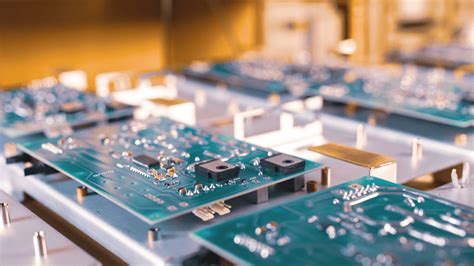
Printed Circuit Boards (PCBs) are the backbone of modern electronics, found in everything from smartphones to industrial machinery. However, designing and manufacturing a PCB is only half the battle. Once a PCB is assembled, it often requires debugging to ensure it functions as intended. Debugging a PCB can be a complex and time-consuming process, but with the right techniques and tools, it can be made more manageable. This article will explore various PCB debugging techniques, from basic visual inspections to advanced methods using specialized equipment.
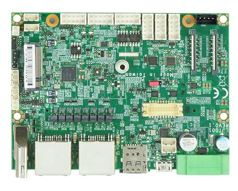
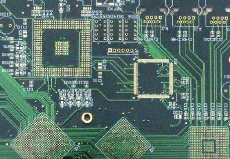
1. Visual Inspection
The first step in debugging any PCB is a thorough visual inspection. This may seem rudimentary, but many issues can be identified simply by looking at the board.
1.1 Check for Physical Damage
Inspect the PCB for any visible signs of damage, such as cracks, burns, or broken traces. Components that appear discolored or charred may indicate overheating or short circuits.
1.2 Verify Component Placement
Ensure that all components are correctly placed and oriented. Misplaced or incorrectly oriented components, such as diodes or capacitors, can cause the circuit to malfunction.
1.3 Inspect Solder Joints
Poor solder joints are a common cause of PCB failures. Look for cold solder joints, solder bridges, or insufficient solder. A magnifying glass or microscope can be helpful for this step.
1.4 Check for Foreign Objects
Sometimes, foreign objects like metal shavings or solder balls can cause short circuits. Carefully inspect the board for any debris that may have been left behind during manufacturing.
2. Continuity Testing
Continuity testing is a fundamental technique used to verify that electrical connections are intact. This is typically done using a multimeter.
2.1 Set Up the Multimeter
Set your multimeter to the continuity mode, which usually produces an audible beep when a connection is detected.
2.2 Test Traces and Connections
Place one probe on one end of a trace or connection and the other probe on the other end. If the multimeter beeps, the connection is good. If not, there may be a break in the trace or a bad solder joint.
2.3 Check for Shorts
To check for shorts, place one probe on a ground point and the other on various points in the circuit. If the multimeter beeps where it shouldn’t, there may be an unintended connection to ground.
3. Power-On Testing
Once you’ve confirmed that there are no obvious physical issues or shorts, the next step is to power on the PCB and observe its behavior.
3.1 Use a Current-Limited Power Supply
When powering on the PCB for the first time, use a current-limited power supply to prevent damage in case of a short circuit. Gradually increase the current limit while monitoring the voltage.
3.2 Measure Voltages
Use a multimeter to measure the voltages at various points in the circuit, such as power supply pins, voltage regulators, and ICs. Compare these measurements to the expected values from the schematic.
3.3 Check for Overheating
After powering on the PCB, quickly scan the board for any components that are overheating. Overheating can indicate a short circuit, incorrect component values, or excessive current draw.
4. Signal Tracing
Signal tracing involves following the flow of signals through the circuit to identify where they deviate from expected behavior.
4.1 Use an Oscilloscope
An oscilloscope is an invaluable tool for signal tracing. It allows you to visualize the waveform of a signal and measure its amplitude, frequency, and timing.
4.2 Start at the Input
Begin at the input of the circuit and work your way through, checking the signal at each stage. Compare the observed signals to the expected waveforms from the schematic.
4.3 Check Clock Signals
If your circuit includes a microcontroller or other clocked device, verify that the clock signal is present and within the expected frequency range.
4.4 Look for Signal Distortion
Distorted signals can indicate issues such as impedance mismatches, poor grounding, or faulty components. Use the oscilloscope to identify and diagnose these problems.
5. Component Testing
Individual components can fail or be incorrectly specified, leading to circuit malfunctions. Testing components can help isolate the problem.
5.1 Test Passive Components
Use a multimeter to test resistors, capacitors, and inductors. Compare the measured values to the expected values from the schematic.
5.2 Test Diodes and Transistors
Diodes and transistors can be tested using the diode mode on a multimeter. For transistors, check the base-emitter and base-collector junctions.
5.3 Test Integrated Circuits (ICs)
Testing ICs can be more challenging, but some basic checks can be performed. Verify that the power supply pins are receiving the correct voltage and that the input and output pins are behaving as expected.
5.4 Use a Component Tester
A dedicated component tester can quickly identify faulty components and provide detailed information about their characteristics.
6. Thermal Imaging
Thermal imaging can be a powerful tool for identifying overheating components or areas of the PCB that are drawing excessive current.
6.1 Use a Thermal Camera
A thermal camera can visualize the temperature distribution across the PCB. Hotspots can indicate components that are failing or operating outside their specified parameters.
6.2 Identify Thermal Anomalies
Compare the thermal image to the expected heat distribution based on the circuit design. Unexpected hotspots may indicate a short circuit, incorrect component values, or poor thermal management.
6.3 Monitor Over Time
In some cases, thermal issues may only become apparent after the PCB has been powered on for some time. Monitor the thermal image over time to identify any gradual increases in temperature.
7. Boundary Scan Testing
Boundary scan testing, also known as JTAG testing, is a more advanced technique used for debugging complex PCBs, particularly those with multiple ICs.
7.1 Understand the JTAG Interface
The JTAG (Joint Test Action Group) interface is a standard for testing and debugging PCBs. It allows you to control and observe the state of individual pins on an IC.
7.2 Use Boundary Scan Software
Boundary scan software can automate the process of testing and debugging. It can identify issues such as open circuits, short circuits, and incorrect component values.
7.3 Test Interconnections
Boundary scan testing is particularly useful for verifying the interconnections between ICs on a PCB. It can identify issues such as broken traces or incorrect wiring.
8. Firmware and Software Debugging
In many modern PCBs, the hardware is controlled by firmware or software. Debugging these elements is often necessary to resolve issues.
8.1 Check for Firmware Bugs
If your PCB includes a microcontroller or FPGA, ensure that the firmware is functioning correctly. Use debugging tools such as breakpoints, watchpoints, and logging to identify and fix bugs.
8.2 Verify Communication Protocols
If your PCB communicates with other devices, verify that the communication protocols (e.g., I2C, SPI, UART) are functioning correctly. Use a logic analyzer to capture and analyze the communication signals.
8.3 Update Firmware
In some cases, updating the firmware to the latest version can resolve issues. Ensure that the firmware is compatible with the hardware and that any known bugs have been addressed.
9. Environmental Testing
Environmental factors such as temperature, humidity, and vibration can affect the performance of a PCB. Testing under different environmental conditions can help identify issues that may not be apparent under normal conditions.
9.1 Temperature Testing
Test the PCB at different temperatures to ensure that it operates correctly across its specified temperature range. Use a temperature chamber to simulate different environmental conditions.
9.2 Humidity Testing
High humidity can cause issues such as corrosion or short circuits. Test the PCB in a humid environment to ensure that it is properly sealed and protected.
9.3 Vibration Testing
If the PCB will be used in a high-vibration environment, such as an automotive application, perform vibration testing to ensure that components and solder joints can withstand the stress.
10. Documentation and Collaboration
Effective debugging often requires collaboration and thorough documentation.
10.1 Document Your Findings
Keep detailed records of your debugging process, including the steps you’ve taken, the results of your tests, and any issues you’ve identified. This documentation can be invaluable for future debugging efforts.
10.2 Collaborate with Others
If you’re working as part of a team, collaborate with others to share findings and insights. Different team members may have different areas of expertise, and collaboration can lead to more effective debugging.
10.3 Review the Schematic and Layout
Sometimes, issues can be traced back to errors in the schematic or PCB layout. Review these documents carefully to ensure that they are accurate and that there are no design flaws.
Conclusion
Debugging a PCB is a multifaceted process that requires a combination of technical skills, the right tools, and a systematic approach. From basic visual inspections to advanced techniques like boundary scan testing, each method plays a crucial role in identifying and resolving issues. By following the techniques outlined in this article, you can streamline the debugging process and ensure that your PCB functions as intended. Remember, patience and attention to detail are key—debugging can be challenging, but with the right approach, even the most complex issues can be resolved.