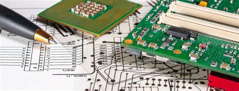
PCB Debugging Techniques: A Comprehensive Guide
Printed Circuit Boards (PCBs) are the backbone of modern electronics, serving as the platform for interconnecting various electronic components. However, designing and manufacturing a PCB is only half the battle. The real challenge often lies in debugging the PCB to ensure it functions as intended. Debugging a PCB can be a daunting task, especially when dealing with complex designs and high-density components. This article aims to provide a comprehensive guide to PCB debugging techniques, covering both traditional methods and modern tools that can help engineers identify and resolve issues efficiently.
1. Understanding the Basics of PCB Debugging
Before diving into specific debugging techniques, it’s essential to understand the fundamental principles of PCB debugging. Debugging is the process of identifying, isolating, and resolving issues that prevent a PCB from functioning correctly. These issues can range from simple soldering defects to complex signal integrity problems.
1.1 Common PCB Issues
- Open Circuits: These occur when there is a break in the conductive path, preventing current from flowing through the circuit.
- Short Circuits: These happen when two or more conductive paths that should not be connected come into contact, causing unintended current flow.
- Component Failures: Individual components may fail due to manufacturing defects, overheating, or other factors.
- Signal Integrity Issues: These include problems like crosstalk, reflections, and electromagnetic interference (EMI) that can distort signals and affect the performance of the PCB.
- Power Supply Issues: Problems with the power supply, such as voltage drops or noise, can cause the PCB to malfunction.
1.2 Debugging Tools and Equipment
To effectively debug a PCB, you need the right tools and equipment. Some of the most commonly used tools include:
- Multimeter: A versatile tool for measuring voltage, current, and resistance.
- Oscilloscope: Used to visualize and analyze electrical signals over time.
- Logic Analyzer: Helps in debugging digital circuits by capturing and displaying multiple signals simultaneously.
- Thermal Camera: Useful for identifying overheating components.
- Spectrum Analyzer: Used to analyze the frequency spectrum of signals, helping to identify EMI issues.
- Soldering Iron and Desoldering Tools: Essential for repairing soldering defects or replacing faulty components.
2. Visual Inspection
The first step in debugging a PCB is a thorough visual inspection. Many issues can be identified simply by looking at the board.
2.1 Check for Physical Damage
Inspect the PCB for any visible signs of damage, such as cracks, burns, or broken traces. Physical damage can often be the root cause of circuit failures.
2.2 Inspect Soldering Joints
Poor soldering is a common cause of PCB issues. Look for cold solder joints, solder bridges, or insufficient solder. A magnifying glass or microscope can be helpful for this task.
2.3 Verify Component Placement
Ensure that all components are correctly placed and oriented. A misplaced or incorrectly oriented component can cause the circuit to fail.
2.4 Check for Foreign Objects
Sometimes, foreign objects like solder balls, dust, or metal shavings can cause short circuits. Carefully inspect the PCB for any such objects and remove them if found.
3. Electrical Testing
Once the visual inspection is complete, the next step is to perform electrical testing to identify any hidden issues.
3.1 Continuity Testing
Use a multimeter to check for continuity between different points on the PCB. This helps identify open circuits or broken traces. Ensure that all connections that should be continuous are indeed continuous, and those that should not be connected are not.
3.2 Resistance Measurement
Measure the resistance across various components and traces to ensure they are within the expected range. Abnormal resistance values can indicate issues like short circuits or faulty components.
3.3 Voltage Measurement
Measure the voltage at different points on the PCB, especially around power supply components. Compare the measured values with the expected values from the schematic. Any significant deviation could indicate a problem with the power supply or related components.
3.4 Current Measurement
In some cases, measuring the current flowing through specific parts of the circuit can help identify issues like short circuits or excessive power consumption.
4. Signal Integrity Analysis
Signal integrity issues can be challenging to diagnose, but they are critical for the proper functioning of high-speed digital circuits.
4.1 Oscilloscope Analysis
Use an oscilloscope to visualize the signals on the PCB. Look for anomalies like ringing, overshoot, undershoot, or signal distortion. These issues can often be resolved by adjusting trace lengths, adding termination resistors, or improving the power supply decoupling.
4.2 Crosstalk Analysis
Crosstalk occurs when signals from one trace interfere with adjacent traces. To minimize crosstalk, ensure that high-speed signals are routed away from each other and use ground planes to shield sensitive traces.
4.3 Reflections and Impedance Matching
Reflections can occur when there is a mismatch in impedance between the source, transmission line, and load. Use impedance matching techniques, such as adding series resistors or using controlled impedance traces, to minimize reflections.
4.4 EMI Testing
Electromagnetic interference (EMI) can cause signal integrity issues and affect the performance of the PCB. Use a spectrum analyzer to identify sources of EMI and take steps to mitigate them, such as adding shielding or filtering components.
5. Thermal Analysis
Overheating is a common issue in PCBs, especially in high-power applications. Thermal analysis helps identify components that are running too hot and may fail prematurely.
5.1 Thermal Imaging
Use a thermal camera to capture images of the PCB while it is operating. Look for hotspots that indicate components or traces that are overheating.
5.2 Thermal Profiling
Perform a thermal profile of the PCB by measuring the temperature at various points over time. This helps identify components that may be operating outside their specified temperature range.
5.3 Heat Dissipation Techniques
If overheating is identified, consider implementing heat dissipation techniques such as adding heat sinks, improving airflow, or using thermal vias to conduct heat away from critical components.
6. Functional Testing
Functional testing involves verifying that the PCB performs its intended function correctly.
6.1 Power-On Testing
Power on the PCB and observe its behavior. Check for any abnormal behavior such as unexpected resets, failure to boot, or incorrect output signals.
6.2 Firmware and Software Debugging
If the PCB includes a microcontroller or other programmable components, ensure that the firmware or software is functioning correctly. Use debugging tools like JTAG or SWD to step through the code and identify any issues.
6.3 Boundary Scan Testing
Boundary scan testing is a technique used to test the interconnections between integrated circuits on a PCB. It is particularly useful for testing complex, high-density boards where physical access to all nodes is difficult.
7. Advanced Debugging Techniques
For more complex issues, advanced debugging techniques may be required.
7.1 X-Ray Inspection
X-ray inspection allows you to see inside the PCB and inspect solder joints, vias, and other internal structures that are not visible to the naked eye. This is particularly useful for identifying issues like voiding in solder joints or misaligned components.
7.2 Time-Domain Reflectometry (TDR)
TDR is a technique used to locate faults in transmission lines by sending a pulse down the line and analyzing the reflected signal. It is useful for identifying issues like open circuits, short circuits, or impedance mismatches.
7.3 Scanning Electron Microscopy (SEM)
SEM provides high-resolution images of the PCB surface, allowing for detailed inspection of solder joints, traces, and components. It is particularly useful for identifying microscopic defects that may be causing issues.
7.4 Failure Analysis
If a component fails, performing a failure analysis can help determine the root cause. This may involve techniques like decapsulation, cross-sectioning, or chemical analysis to identify the failure mechanism.
8. Best Practices for PCB Debugging
To ensure efficient and effective debugging, follow these best practices:
8.1 Document Everything
Keep detailed records of all tests, measurements, and observations. This documentation can be invaluable for identifying patterns or recurring issues.
8.2 Start with the Basics
Always start with the simplest and most obvious checks, such as visual inspection and continuity testing, before moving on to more complex techniques.
8.3 Use a Systematic Approach
Follow a systematic approach to debugging, starting with power supply issues, then moving on to signal integrity, and finally functional testing. This helps ensure that you don’t overlook any potential issues.
8.4 Collaborate with Others
Debugging can be a challenging and time-consuming process. Don’t hesitate to collaborate with colleagues or seek advice from online communities. Fresh perspectives can often lead to new insights.
8.5 Stay Updated
The field of electronics is constantly evolving, with new tools and techniques being developed all the time. Stay updated on the latest advancements in PCB debugging to ensure you are using the most effective methods.
9. Conclusion
Debugging a PCB is a critical step in the development of any electronic device. While it can be a complex and challenging process, following a systematic approach and using the right tools and techniques can help you identify and resolve issues efficiently. By understanding the common issues that can arise, performing thorough visual and electrical inspections, and utilizing advanced debugging techniques when necessary, you can ensure that your PCB functions as intended and meets the required performance standards.
Remember, debugging is not just about fixing problems; it’s also about learning from them. Each debugging session provides valuable insights that can help improve your design and manufacturing processes, leading to more reliable and robust PCBs in the future.